Digital Comparator
The Digital Comparator compares two digital buses and outputs the comparison results on the five output pins. The device outputs the five combinatorial possibilities, allowing the user to easily see the results of the comparison. The bus inputs can have between 2 and 32 bits, and can be formatted as unsigned, offset binary, or two's complement.
For a comparator with analog inputs and digital outputs, see the Comparator with Analog Inputs and Digital Outputs topic.
In this topic:
| Model Name: | Digital Comparator | |||
| Simulator: | This device is compatible with the SIMPLIS simulator. | |||
| Parts Selector Menu Location: | ||||
| Symbol Library: | None - the symbol is automatically generated when placed or edited. | |||
| Model Library: | None - the model is automatically generated when the simulation is run. | |||
| Subcircuit Names: |
|
|||
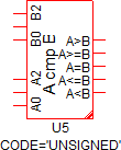
| Symbol: |
|
|||
| Multiple Selections: | Only one device at a time can be edited. | |||
Editing the Digital Comparator
To configure the Digital Comparator, follow these steps:
- Double click the symbol on the schematic to open the editing dialog to the Parameters tab.
- Make the appropriate changes to the fields described in the table below the image.
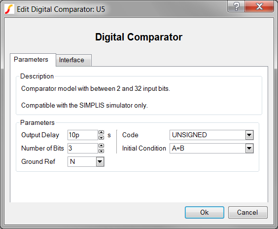
| Label | Parameter Description |
| Propagation Delay | Delay from when the input state changes until the output changes |
| Number of Bits | Number of input bits to the Digital Comparator |
| Ground Ref | Determines whether or not a device has a ground reference pin. Any digital component that has an input or output pin connected to an analog circuit node must have its Ground Ref pin connected to an analog node. This is usually the ground on the schematic. |
| Code | Encoding scheme for binary inputs/outputs for the Digital Comparator |
| Initial Condition | Initial condition of the Digital Comparator output at time=0 |
To define the parameters for the interface between this digital component and each analog component connected directly to an input or output pin, follow these steps:
- From the Edit Digital Comparator dialog box, click on the Interface tab.
- Make the appropriate changes to the fields described in the table below the image.
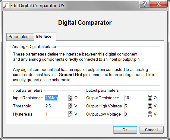
| Label | Parameter Description | |||||||
| Input Resistance | Input resistance of each Digital Comparator input pin | |||||||
| Hysteresis, Threshold | 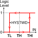 |
Hysteresis and
Threshold of the inputs. The hysteretic-window width, HYSTWD
is centered around Threshold (TH) voltage. To
determine the actual threshold ( TL , THI ),
substitute Threshold (TH) and Hysteresis
(HYSTWD) in each of the following formulas:
|
||||||
| Output Resistance | Output resistance of each Digital Comparator output pin | |||||||
| Output High Voltage | Output high voltage for each Digital Comparator output pin | |||||||
| Output Low Voltage | Output low voltage for each Digital Comparator output pin | |||||||
Examples
An example using the Digital Comparator is a up/down counter with programmable limits. This example is described in the Other Counters.
Subcircuit Parameters
Because the Digital Comparator model is generated by a template script when the simulation is executed, a hand-coded model cannot be inserted into a netlist. The template script for this device is simplis_make_adder_model.sxscr, which licensed users can download as part of a zip archive of all built-in scripts.
To download the zip archive, follow these steps:
- Click http://www.simetrix.co.uk/simetrix80/scripts.zip to download the script archive.
- Enter the user name and password you received with your license file.
The following parameter table defines the parameters used in this model.
| Parameter Name | Label | Data Type | Range | Units | Parameter Description | |||||||
| CODE | Code | String |
|
none | Encoding scheme for binary inputs/outputs for the Digital Comparator | |||||||
| GNDREF | Ground Ref | String |
|
none | Determines whether or not a device has a ground reference pin. Any digital component that has an input or output pin connected to an analog circuit node must have its Ground Ref pin connected to an analog node. This is usually the ground on the schematic. | |||||||
| HYSTWD, TH |
Hysteresis, Threshold |
Number | min: 1f | V | |
Hysteresis and Threshold of
the inputs. The hysteretic-window width, HYSTWD is centered around
Threshold (TH) voltage. To determine the actual threshold (
TL , THI ), substitute Threshold (TH) and
Hysteresis (HYSTWD) in each of the following formulas:
|
||||||
| IC | Initial Condition | Number |
|
none | Initial condition of the Digital Comparator output at time=0 | |||||||
| NUMBITS | Number of Bits | Integer | none | Number of input bits to the Digital Comparator | ||||||||
| OUT_DELAY | Propagation Delay | Number | 1f to 1024 | s | Delay from when the input state changes until the output changes | |||||||
| RIN | Input Resistance | Number | min: 100 | Ω | Input resistance of each Digital Comparator input pin | |||||||
| ROUT | Output Resistance | Number | min: 1m | Ω | Output resistance of each Digital Comparator output pin | |||||||
| VOH | Output High Voltage | Number | any | V | Output high voltage for each Digital Comparator output pin | |||||||
| VOL | Output Low Voltage | Number | any | V | Output low voltage for each Digital Comparator output pin | |||||||