Application F - Combining a SIMPLIS schematic with a C-code DLL
This application topic demonstrates how a C-code DLL can be interfaced with a Simplis schematic. The example used is a valley switching flyback in which the primary switch turns on when the voltage across the switch is at a local minimum point, or valley, of the resonant ringing which occurs in discontinuous mode operation. Many designs dynamically change which valley point in the resonant ringing waveform the switch is turned on based on circuit operating conditions. The example here uses a C-code DLL implementation of the algorithm that determines at which of the valleys the switching will occur.
The C-code DLL can be useful in many ways. If, in the longer term, it is intended to implement the algorithm in hardware, the DLL may be able to model the algorithm much more quickly than by designing gate-level circuitry. Various algorithms can be investigated by writing a few lines of code rather than generating and debugging a circuit model, which in some cases may be much more complicated. The circuitry can be designed after the best algorithm is decided upon. Alternately, if the intention is use a microcontroller/software to implement the algorithm, the DLL provides a simple way to model this in SIMPLIS.
To download the examples for the Applications Module, click Applications_Examples.zip.
In this topic:
Key Concepts
This topic addresses the following key concepts:
- High level understanding of valley switching
- One method of implementing valley switching
- Advantages of integrating a C-code DLL with the schematic rather than creating a gate-level design of the digital logic functionality
What You Will Learn
In this topic, you will learn the following:
- Definition of Valley Switching
- Advantages of modifying the power switch turn-on point based on line and load conditions
- Use of the input voltage and a control voltage (proportional to peak current) in a PCC flyback as inputs to the DLL
- Use of the C-code DLL to implement the algorithm for changing the switching point
- Typical behavior of the valley switching flyback during load/line changes
Usage of a C-Code DLL in a Valley Switching Example
The model of a 48W, 12V output DC-to-DC converter including valley switching is shown in Figure 1a. A high level view of the IC (U1) schematic is shown in Figure 1b. The design will be examined at 155V and 325V input (approximate rectified DC voltage from line voltages of 110 VAC and 230 VAC, respectively). This discussion will assume basic knowledge of flyback converters with peak current control. Note that, in practical applications, there are typically other features such as burst mode at very light load, but the example here is mainly intended to model the valley switching aspects. The circuit is a peak current control (PCC) flyback with controller IC, U1. The circuitry is typical of many designs: a shunt to sense current, a bias winding to provide IC power, and a TL431 configuration on the output to regulate the voltage. The IC is a typical PCC controller except for one aspect: It feeds a logic signal FBTH3:0 to U4, which is defined by a C-code DLL. The logic signal FBTH3:0 indicates the level of the feedback signal FB. The DLL implements an algorithm to control the output NSZX3:0 which controls the manner in which the IC will turn on the power switch. More detail will follow in the next sections.
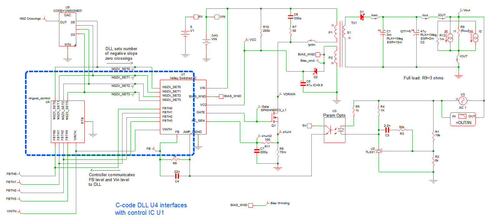 Figure 1a. Typical flyback converter model with added C-code
DLL.
Figure 1a. Typical flyback converter model with added C-code
DLL.
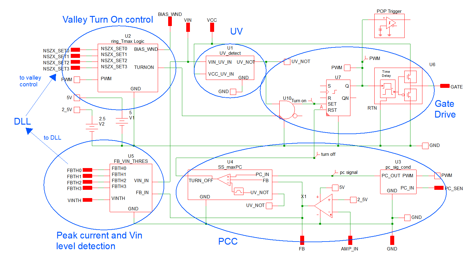 Figure 1b.
High level details of the IC U1.
Figure 1b.
High level details of the IC U1.
Background of Valley Switching
Many high voltage applications operate in discontinuous mode to minimize turn-on loss and
EMI. Figure 2 below shows typical primary and secondary currents and the switch voltage and
the classic resonant ring of the drain voltage after the secondary current deceases to zero.
Turn-on at point A is desirable because it minimizes RMS current in discontinuous mode, but
turn-on at point B (the "valley") greatly reduces the CV2 loss due to discharge
of the parasitic and snubber capacitances associated with the power switch. Switching at
point B is called valley switching and is attractive in higher voltage applications where
the CV2 loss can be significant.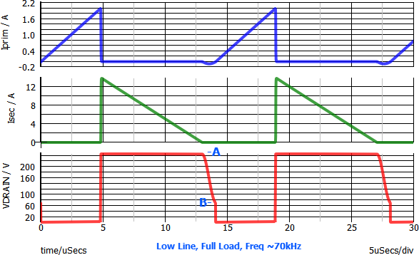 Figure 2. Primary and secondary current
and the switch (drain) voltage at low line, full load. Switching at point B is called
valley switching and greatly reduces the switching losses due to capacitive
discharge.
Figure 2. Primary and secondary current
and the switch (drain) voltage at low line, full load. Switching at point B is called
valley switching and greatly reduces the switching losses due to capacitive
discharge.
If switching always occurs at the valley of the first resonant ring, the switching
frequency will increase with increasing line and decreasing load, increasing the
CV2 loss and diminishing the gains from valley switching. Figures 3 and 4 show
the increase in frequency from 70kHz in Figure 2 to 100kHz at the higher line and 365kHz at
light load.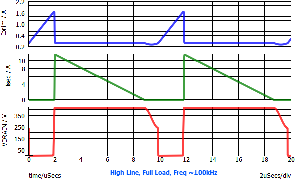 Figure 3. Primary and
secondary current and the switch (drain) voltage at low line, full load. Switching at
point B is called valley switching and greatly reduces the switching losses due to
capacitive discharge.
Figure 3. Primary and
secondary current and the switch (drain) voltage at low line, full load. Switching at
point B is called valley switching and greatly reduces the switching losses due to
capacitive discharge.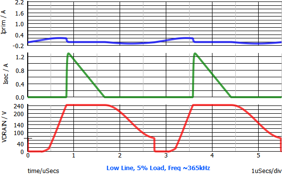 Figure 4. Low line, 5% load
waveforms.
Figure 4. Low line, 5% load
waveforms.
This has driven designers of valley switching converters to develop schemes where the switching occurs at a different valley during the resonant ringing. The valley selection can be varied based on an algorithm related to line and load. For example, under the same conditions as figures 3 and 4 above, the switching frequency is changed back to the ~70kHz range by switching at the 2nd valley and the 6th valley. See figures 5 and 6 below.
Note that the peak and RMS currents are higher when switching at a valley later in the
resonance. So there will be a tradeoff between the increased I2R loss and reduced
switching loss. Note that the increase in peak current here will be an important factor in
the method of control described later.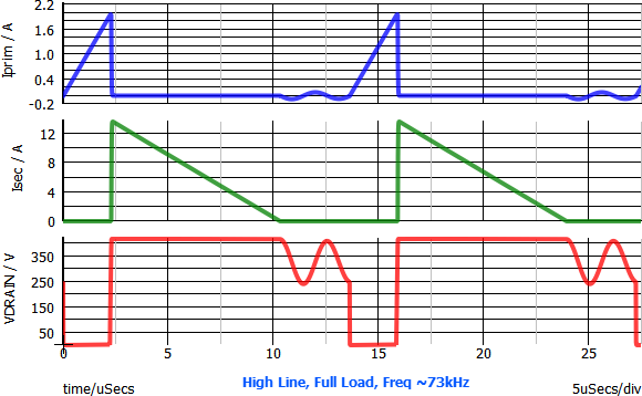 Figure 5. High line, full load with switching
at valley 2.
Figure 5. High line, full load with switching
at valley 2.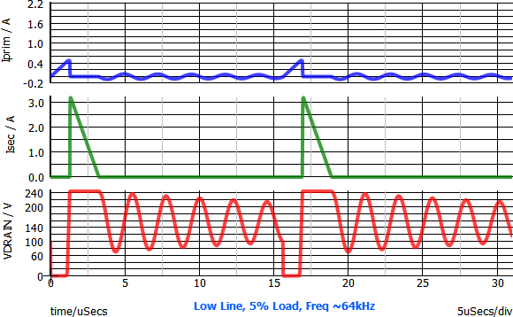 Figure 6. Low line, 5%
load with switching at valley 6.
Figure 6. Low line, 5%
load with switching at valley 6.
Method of Switching at the Valley
In our example, the controller bias is generated by a commonly used technique: a flyback
bias winding on the main transformer. The waveform is shown in the Figures 7 & 8 below.
Using this winding to control the timing of the valley switching is convenient in a
practical application: the center of the resonant ringing amplitude is at zero volts and the
valley is 1/4 of the resonant ringing period after the zero crossing with a negative slope.
(Going forward, we will call this an "NSZ crossing" for "negative slope zero crossing".) The
sub circuit shown in figure 9 counts the number of NSZ crossings and when they equal the
number specified by the DLL, the TURNON signal will transition to "1" after the 1/4 cycle
delay. 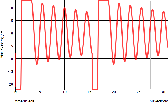 Figure 7. Bias winding
voltage.
Figure 7. Bias winding
voltage.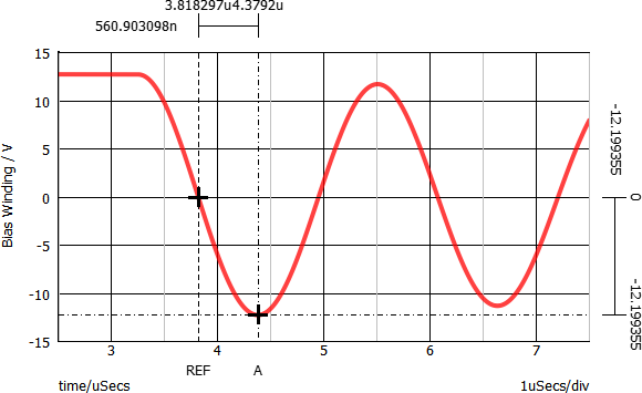 Figure 8: Bias
winding: 1/4 cycle from NSZ crossing to valley.
Figure 8: Bias
winding: 1/4 cycle from NSZ crossing to valley.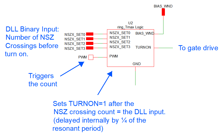 Figure 9. Valley control subcircuit that determines turn on of
main switch. (Details in the schematic.)
Figure 9. Valley control subcircuit that determines turn on of
main switch. (Details in the schematic.)
Input to the DLL: Peak Current and Input Voltage Levels
Figure 10 shows typical control waveforms typical for a PCC flyback. The shunt voltage is
at the top and the voltage after signal conditioning (blanking, RC filtering, amplification
and level-shifting) is shown at the bottom. The feedback (FB) signal controls the peak of
the conditioned signal. This peak is limited to 1V (red trace).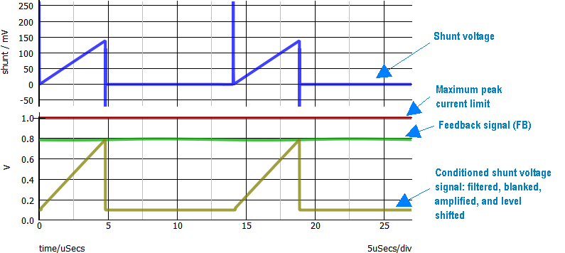 Figure 10. Shunt voltage
(top, blue), conditioned shunt voltage (yellow), feedback signal (green), and peak current
limit (red).
Figure 10. Shunt voltage
(top, blue), conditioned shunt voltage (yellow), feedback signal (green), and peak current
limit (red).
In our example circuit, the feedback signal is compared to 4 threshold levels REF-FB3:0 as
shown in figure 11. Each of the FBTHx outputs will transition to 1 when FB exceeds its
respective threshold. FB0 has the lowest threshold, FB3 the highest, there are only 5
different states of FBTH3:0. FBTH3:0 is fed to the DLL. In this way, a quantized indication
FBTH3:0 of the level of the peak current (proportional to FB) is sent to the DLL. The DLL is
also sent a signal indicating whether the input voltage low or high line (not shown
here).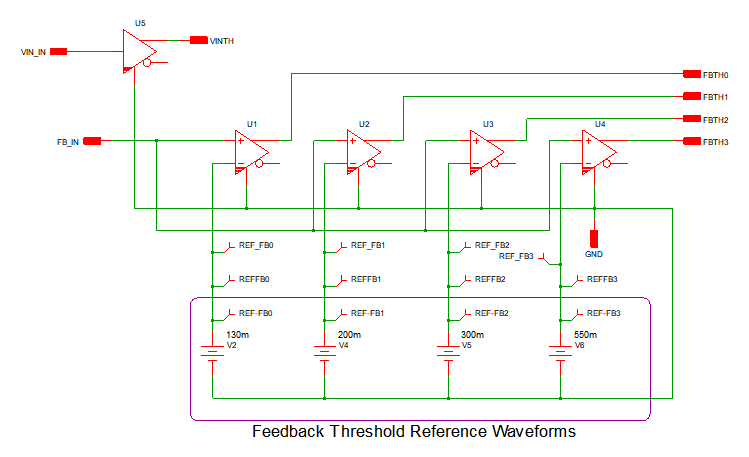 Figure 11. Feedback (FB) Threshold Comparison Circuit.
C-Code DLL Interface and Dialog Box
The circuit interface from the control IC to the DLL is shown in Figure 12. Inputs FBTH3:0
and the high/low line indicator VINTH are fed as input to the DLL. During each wake event,
the DLL runs the algorithm and the output NSZX3:0 is provided to the IC U1 to specify the
number of NSZ crossings. The dialog box in Figure 13 shows the input settings for the
algorithm which can be changed without modifying the code.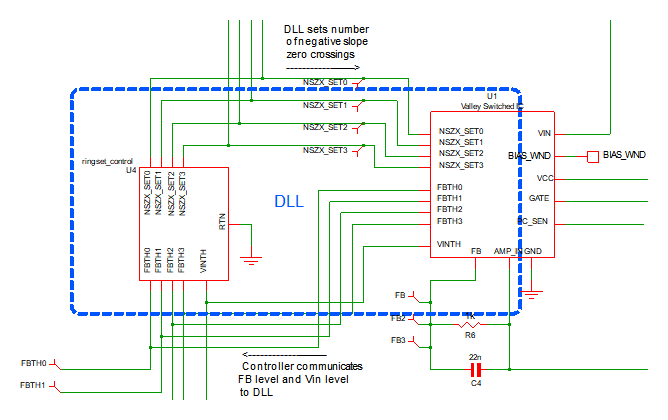 Figure 12. Communication
between the control IC and the DLL.
Figure 12. Communication
between the control IC and the DLL.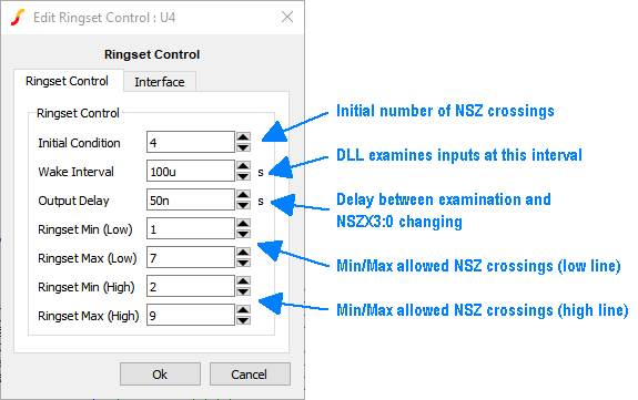 Figure 13. The DLL dialog box.
C-Code DLL Algorithm to Set the Number of Negative Slope Zero (NSZ) Crossings
Using a C-code DLL early in the design phase allows the designer to easily iterate the
valley switching algorithm and compare a number of different approaches. Simple
modifications like changing the increment or decrement amounts require simply changing a
line of code. If we want to change the number of threshold levels, we can copy and paste the
circuitry in Figure 11 and add some code. If we want to change the algorithm to respond to
average current in addition to peak current, we could add more inputs and modify the code as
needed. If we want to react to the current in a more complex manner using an actual current
reading rather than a level, we could use an ADC to feed the measured current reading into
the DLL. In any case, the coding change is likely much faster to implement than changing
circuitry. If the functions are to be implemented in a microcontroller, the C-code DLL is a
better way to simulate the eventual design.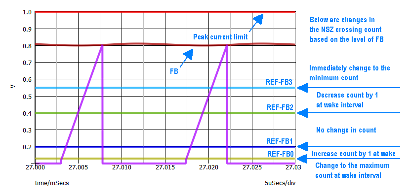 Figure 14. Algorithm
implemented by the DLL.
Figure 14. Algorithm
implemented by the DLL.
Understanding the Transition in NSZ Count
Figures 15 and 17 show the control and power train waveforms for the circuit at low line
and a light load when the NSZ count is 1. Feedback FB is between REF-FB0 and REF-FB1 which,
at the next wake event, will result in an increase the NSZ crossing count to 2. Figures 16
and 18 show the result after the increase in count from 1 to 2. The frequency reduces and
the resultant FB signal (and peak current) increases. The peak current comes to steady state
between REF-FB1 and REF-FB2 where the algorithm specifies no further change.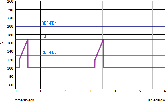 Figure 15. FB in a range that requires NSZ
crossing increased.
Figure 15. FB in a range that requires NSZ
crossing increased.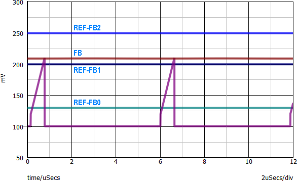 Figure 16. After
increase, FB is in the "no change" range.
Figure 16. After
increase, FB is in the "no change" range.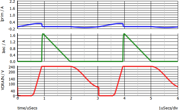 Figure 17. Power train waveforms for figure
15.
Figure 17. Power train waveforms for figure
15.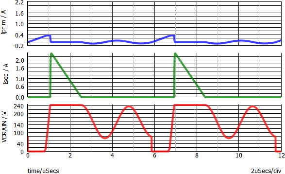 Figure 18. Power train
waveforms for figure 16.
Figure 18. Power train
waveforms for figure 16.
Examples of Dynamic Circuit Behavior
Below are some simulation examples demonstrating behavior under various line and load
change conditions. The grid at the bottom plots the number of NSZ crossings demanded by the
DLL, determining at which valley the switching will occur.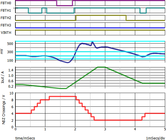 Figure 19. Slow load change at high
line: There is gradual change in number of NSZ crossings as the feedback signal reacts to
load changes. The min and max number of NSZ crossings are defined by the C-code DLL dialog
box.
Figure 19. Slow load change at high
line: There is gradual change in number of NSZ crossings as the feedback signal reacts to
load changes. The min and max number of NSZ crossings are defined by the C-code DLL dialog
box.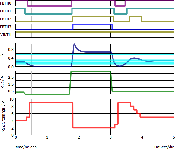 Figure 20. Same as
figure 19, but with faster load steps and larger load steps at 1.7ms and 3ms. The number
of NSZ crossings change faster in response.
Figure 20. Same as
figure 19, but with faster load steps and larger load steps at 1.7ms and 3ms. The number
of NSZ crossings change faster in response.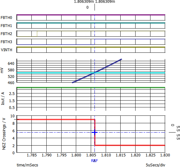 Figure 21: Zooming in on Figure 20 at
the load step at 1.7ms. Note immediate change in the ring count as FB crosses the REF-FB3.
This is critical since the converter cannot support full load with a high number of NSZ
crossings.
Figure 21: Zooming in on Figure 20 at
the load step at 1.7ms. Note immediate change in the ring count as FB crosses the REF-FB3.
This is critical since the converter cannot support full load with a high number of NSZ
crossings.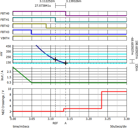 Figure 22. Zooming in
on Figure 20 at the load step at 3ms. FB is below REF-FB1 at one wake event and increases
NSZ crossing count by 1. At the next wake event, FB is below REF-FB0 and jumps to the max
NSZ crossing count. FB crosses the lowest threshold early in the wake cycle(~3.14μS), but
the count does not change until the next wake event.
Figure 22. Zooming in
on Figure 20 at the load step at 3ms. FB is below REF-FB1 at one wake event and increases
NSZ crossing count by 1. At the next wake event, FB is below REF-FB0 and jumps to the max
NSZ crossing count. FB crosses the lowest threshold early in the wake cycle(~3.14μS), but
the count does not change until the next wake event.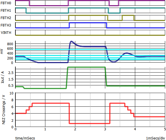 Figure 23. Same as Figure 20, but at low
line. The behavior is similar, but the min and max # of NSZ crossings are different since
they are defined separately in the dialog box.
Figure 23. Same as Figure 20, but at low
line. The behavior is similar, but the min and max # of NSZ crossings are different since
they are defined separately in the dialog box.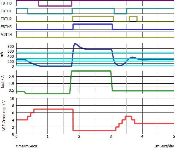 Figure 24: same as Figure 23, but the
FB0 threshold has been reduced and FB does not cross it, so the NSZ crossings count at
~3.1ms increases 1 step at a time instead of jumping to the max count.
Figure 24: same as Figure 23, but the
FB0 threshold has been reduced and FB does not cross it, so the NSZ crossings count at
~3.1ms increases 1 step at a time instead of jumping to the max count.
The C-Code DLL Implementation: Specification
To create the DLL that implements the algorithm that sets the number of Negative Slope Zero (NSZ) crossings, the automatic code generation features were used. A project was created for a device meeting the following specification.
Input Buses:
- CLK (1-bit) (unused in the algorithm, leaves room for future expansion)
- FBTH (4-bit) (feedback threshold pins 0-3)
- VINTH (1-bit) (VIN threshold, 0 for low line condition, 1 for high line condition)
- RSET (4-bit) (renamed NSZX_SET pins 0-3 on the top-level schematic)
- IC: (unsigned integer) the initial condition of the output bus NSZX_SET, default is 1.
- RSET_MIN_LL: (unsigned integer) the minimum number of negative-slope zero crossings at the low line condition, default is 1.
- RSET_MAX_LL: (unsigned integer) the maximum number of negative-slope zero crossings at the low line condition, default is 7.
- RSET_MIN_HL: (unsigned integer) the minimum number of negative-slope zero crossings at the high line condition, default is 3.
- RSET_MAX_HL: (unsigned integer) the maximum number of negative-slope zero crossings at the high line condition, default is 9.
- WAKE_INTERVAL: (double) the DLL-defined digital device will wake up on this interval to see if any changes to the output need to be made, default is 10ms.
- OUTPUT_DELAY: (double) the output delay of the device, default is 50ns.
The C-code DLL Implementation: Code
All SIMPLIS DLL-defined Digital devices need to implement the following functions:
- Setup: where any instantiation and housekeeping items can be dealt with
- Initial Conditions: where the author sets the value of the output buses at t=0 and can request that the device be woken up after a specified delay
- Action: where the behavior of the device during simulation is detailed
- Teardown: where any cleanup can be performed after simulation is complete
During the syntax checking portion of the simulation run, SIMPLIS will locate the DLL, instantiate the necessary data structures that underpin it, then copy in the reference-designator-specific user parameters, customizing it from the defaults for each run. At that point, the Setup function is called. Once setup is complete, SIMPLIS progresses to t=0 where the Initial Conditions routine for each device in the simulation specifies its output values based on users' input. During simulation, the Action function is called every time one of the device's inputs changes, or if the device has previously asked to be awoken. Finally, once simulation completes, the Teardown function is called allowing the DLL author to free any allocated memory and perform any necessary cleanup tasks.
Setup
The project created by the code generation routines includes a number of optional-but-helpful data structures and function definitions. By default, a struct is generated and populated with pointers to the input and output buses and copies of the user input (the parameter values from the schematic). The ringset_control_setup function makes a call to the automatically generated ringset_control_assign_default_pointers function to take advantage of that feature. Some additional code checks the user's values for RSET_MIN_LL/RSET_MAX_LL and RSET_MIN_HL/RSET_MAX_HL to make sure that the minimum values do not exceed the maximum values for each line condition.
Initial Conditions
For devices that have only one output bus and an "IC" parameter that is an unsigned integer, the code generation routines will automatically create a function that reads that user-defined parameter value and assigns it to the output bus. That function, named <project name>_set_initial_condition_single_output_from_IC_parameter must be called explicitly by the code author, however. This project's initial conditions routine, ringset_control_set_initial_condition then does two things:
- calls the auto-generated ringset_control_set_initial_condition_single_output_from_IC_parameter function to specify the value of the output bus RSET at t=0
- requests that the device be woken up at a time equal to t=(0+WAKE_INTERVAL), where the wake interval is a user-configurable parameter
Action
For this example, the action function needs to handle the following every time it wakes up (for an arbitrary t=n):
- determine whether the device is in a low line or high line condition and set the minimum and maximum values accordingly
- read the input bus FBTH into a variable to determine the state of the FBTH0-3 pins
- read the output bus RSET into a variable that is the current number of negative slope zero crossings
- determine the reason that the device is waking up
- schedule the next wake event at t=(n+WAKE_INTERVAL) if the device is active during a
scheduled wake
- If the device is woken up for any reason while FBTH3 is high, the output should be set immediately to the minimum allowed for that line condition. Per the circuit specification, "this is critical since the converter cannot support full load with a high number of NSZ crossings."
- Otherwise, the device ignores input pin changes and instead only operates during its scheduled wake events. When awoken with the pre-determined wake identifier that indicates that this is a scheduled wake event, the device will basically act as a state machine, breaking out of the loop once the first of the below states is found to be true.
- If FBTH2 is high, the output RSET will be decremented until it hits the minimum specified value for the line condition
- If FBTH1 is high, the output RSET will he held constant
- If FBTH0 is high, the output RSET will be incremented until it hits the maximum specified value for the line condition
- If none of the FBTH pins are high, the output RSET will be set to the maximum specified value for the line condition
Regardless of the state, the value to be written to the output RSET will be checked against the minimum and maximum for the line condition and adjusted if necessary.
Teardown
As no explicit raw memory allocation calls were made by the code author and SIMPLIS automatically will free any managed or unmanaged user storage, the Teardown function can be essentially empty.