Comparator with Analog Inputs and Digital Outputs
The Comparator with Analog Inputs and Digital Outputs models a generic comparator with hysteresis. The output of the Comparator is treated as a digital signal for the SIMPLIS event-driven simulator only if the output is connected to SIMPLIS digital devices. If the Comparator output is connected to analog devices, the output voltage levels and output resistance are defined by the Output High Voltage, Output Low Voltage, and the Output Resistance parameters.
There is a finite resistance from each Comparator input to the Comparator ground pin. If you have an application where you require the Comparator to have a true infinite input impedance, you can use a voltage-controlled voltage source (VCVS) to buffer each input pin. Similarly, the outputs of the Comparator have a finite output resistance with a minimum value of 1mΩ. If you require a resistance of less than 1mΩ, you can add a VCVS to the output of the Comparator. The circuit example below demonstrates this technique.
The Hysteresis parameter may never be zero. The minimum parameter value allowed is 1pV. For most applications, this is sufficiently small to be insignificant.
In this topic:
| Model Name: | Comparator with Analog Inputs and Digital Outputs | |||
| Simulator: | This device is compatible with the SIMPLIS simulator. | |||
| Parts Selector Menu Location: | ||||
| Symbol Library: | None - the symbol is automatically generated when placed or edited. | |||
| Model Library: | SIMPLIS_DIGI1.LB | |||
| Subcircuit Name: | SIMPLIS_DIGI1_COMP_Y | |||
| Symbol: |
|
|||
| Multiple Selections: | Only one device at a time can be edited. | |||

Editing the Comparator with Analog Inputs and Digital Outputs
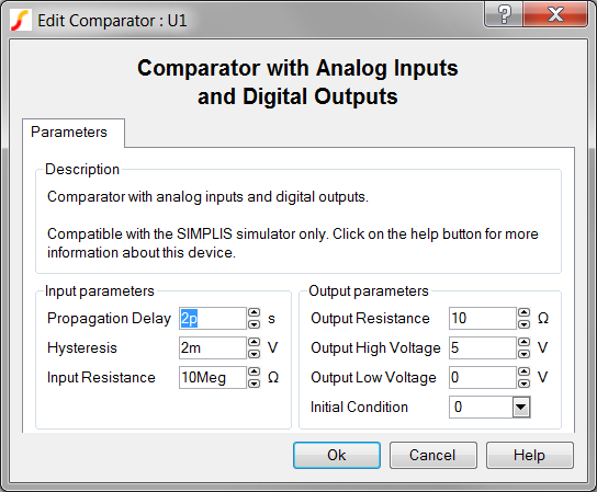
To configure the Comparator with Analog Inputs and Digital Outputs, follow these steps:
- Double click the symbol on the schematic to open the editing dialog to the Parameters tab.
- Make the appropriate changes to the fields described in the table below the image.
| Label | Parameter Description | |||||||
| Propagation Delay | Delay from when any input pin changes state until the outputs change state | |||||||
| Hysteresis | 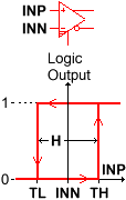 |
The Hysteresis (H) of
the comparator. To determine the actual threshold (TL,
TH), substitute Hysteresis (HYSTWD) in each
of the following formulas, where INN is the negative input
pin voltage. The comparator output voltage will change state when
INP, the positive input pin voltage, reaches TL or
TH :
|
||||||
| Input Resistance | Input resistance of each Comparator input pin | |||||||
| Output Resistance | Output resistance of each Comparator output pin | |||||||
| Output High Voltage | Output high voltage for each Comparator output pin | |||||||
| Output Low Voltage | Output low voltage for each Comparator output pin | |||||||
| Initial Condition | Initial condition of the Comparator output at time=0 | |||||||
Examples
The test circuit used to generate the waveform examples in the next section can be downloaded here: simplis_018_comparator_example.sxsch.
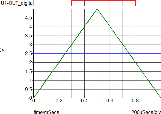
Waveforms
The waveforms below were taken from a Comparator with a 1V Hysteresis parameter, and a slow triangle wave ramp applied to the input. The Comparator output switches from low to high when the ramp reaches 3V and from high to low when the ramp reaches 2V.
Subcircuit Parameters
X$U1 7 9 0 6 8 SIMPLIS_DIGI1_COMP_Y vars: IC=0 RIN=10Meg ROUT=10 HYSTWD=1 VOL=0 VOH=5 DELAY=2p
| Parameter Name | Label | Data Type | Range | Units | Parameter Description | |||||||
| DELAY | Propagation Delay | Number | 1f to 1024 | s | Delay from when any input pin changes state until the outputs change state | |||||||
| GNDREF | Ground Ref | String |
|
none | Determines whether or not a device has a ground reference pin. Any digital component that has an input or output pin connected to an analog circuit node must have its Ground Ref pin connected to an analog node. This is usually the ground on the schematic. | |||||||
| HYSTWD, TH |
Hysteresis, Threshold |
Number | min: 1f | V | 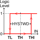 |
Hysteresis and Threshold of
the inputs. The hysteretic-window width, HYSTWD is centered
around Threshold (TH) voltage. To determine the actual
threshold ( TL , THI ), substitute Threshold
(TH) and Hysteresis (HYSTWD) in each of the
following formulas:
|
||||||
| IC | Initial Condition | Number |
|
none | Initial condition of the Inverter/Buffer output at time=0 | |||||||
| RIN | Input Resistance | Number | min: 100 | Ω | Input resistance of each Inverter/Buffer input pin | |||||||
| ROUT | Output Resistance | Number | min: 1m | Ω | Output resistance of each Inverter/Buffer output pin | |||||||
| VOH | Output High Voltage | Number | any | V | Output high voltage for each Inverter/Buffer output pin | |||||||
| VOL | Output Low Voltage | Number | any | V | Output low voltage for each Inverter/Buffer output pin | |||||||