SystemDesigner Data Register
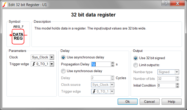
The SystemDesigner Data Register models a clocked digital register. The register can be clocked with any SystemDesigner clock. From the Output parameter box, you can limit the resulting output to either signed or unsigned numbers with fewer than 32 bits.
The propagation delay can be defined as a fixed time, as asynchronous to any clock, or as a synchronous delay where the delay is a number of SystemDesigner -clocks cycles. In this release of SystemDesigner , the synchronous delay is supported only for integer-sampled data simulations.
In this topic:
| Model Name: | SystemDesigner Data Register | |||
| Simulator: | This device is compatible with the SIMPLIS simulator. | |||
| Parts Selector Menu Location: | SystemDesigner Functions (max. 32 bit) | |||
| Symbol Library: | SIMPLIS_SystemDesigner.sxslb | |||
| Model Library: | SIMPLIS_SystemDesigner.lb | |||
| Subcircuit Name: | SIMPLIS_SD_DATA_REG_32 : data register | |||
| Symbol: |
|
|||
| Multiple Selections: | Only one device at a time can be edited. | |||

Editing the SystemDesigner Data Register
To configure the SystemDesigner Data Register, follow these steps:
- Double click the symbol on the schematic to open the editing dialog to the Parameters tab.
- Make the appropriate changes to the fields described in the table below the image.
| Label | Parameter Description |
| Clock source | Specifies the global clock used for the Data Register. The Clock can be set up using the SystemDesigner->Edit SystemDesigner Clocks... menu item or by placing a Start of Conversion Breakin. |
| Trigger edge | Sets the Data Register output to change on specific edges of the Clock:
|
| Use asynchronous delay | Implements a combinatorial model where the output voltage changes in response to the input voltage change after a propagation delay. |
| Propagation delay | The propagation delay from an input change to an output change in seconds. This parameter is used only in models with Asynchronous delay. |
| Use synchronous delay | In response to an input voltage change, the output voltage changes after a designated number of clock cycles. |
| Delay | The propagation delay from an input change to an output change in number of clock cycles. The output will not change until the number of clock cycles has been reached. The output will then change state only on the selected Clock source edges specified by Trigger edge . This parameter is used only in models with Synchronous delay. |
| Clock source | Specifies the global clock used for the Synchronous delay block. The Clock source can be set using the SystemDesigner->Edit SystemDesigner Clocks... menu item or by placing a Start of Conversion Breakin. |
| Trigger edge | Sets the output to change on specific edges of the Clock source:
This parameter is used only in models with Synchronous delay. |
| Use 32 bit signed | The full 32-bit signed data is output. |
| Limit output to: | The output is limited to a Signed or Unsigned number with a designated number of bits. |
| Number type | The output will be limited to either a Signed or Unsigned number if Limit output to is selected.
This parameter is used only in models with Limit output to selected. |
| Number of bits | The limit on the output depends on the Number type parameter:
This parameter is used only in models with Limit output to selected. |
| Initial Condition | Initial condition of the output at time=0. Value is the output bus represented in decimal format. |
Examples
A circuit example using the SystemDesigner register can be downloaded here : simplis_114_systemdesigner_datareg_example.sxsch. In order to simulate this design, follow these steps:
- If you currently have a dialog box open in SIMetrix/SIMPLIS, cancel that dialog box so that the example can open in SIMetrix/SIMPLIS.
- Unzip the archive to a location on your computer.
- To open the schematic, double click the .sxsch file or drag that file into the SIMetrix/SIMPLIS Command Shell.
Waveforms
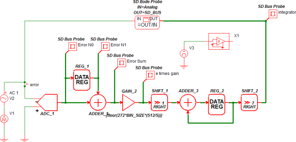
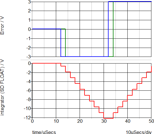
In this example, a complete integrator is implemented using the Data Register REG_1 to store the previous error sample. The function then does the following in this order:
- The integrator uses the trapezoidal rule integration method to integrate the incoming error signal.
- Another register, REG_2, accumulates the result of the previous samples.
- The adder then adds the two analog signals and produces the output: Sum = Error N0 + Error N1.
- The Sum is then gained by the GAIN_1 block and divided by 2 using the shift right operation, SHIFT_1.
- Finally, the accumulator implemented with REG_2 and ADDER_3 stores the accumulated results.
Note the quantization of the integrator output in the integer-type simulations:
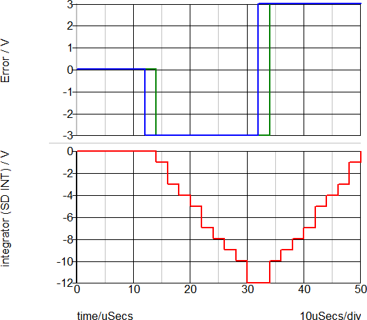
In the floating-point simulation, there is no quantization of the integrated signal.
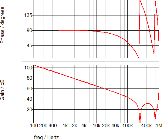
The AC transfer function for the integrator is shown below.