Device Models Used in Simplis
In this topic:
Piecewise-Linear Resistor Models
There are two acceptable model types for piecewise-linear resistors:
- A voltage-defined piecewise-linear resistor, VPWLR
- A current-defined piecewise-linear resistor, IPWLR
.MODEL  mname  mtype  NSEG=k  X0=x0  Y0=y0
+ X1=x1  Y1=y1  X2=x2  Y2=y2 ...  Xk=xk  Yk=yk
where
| .MODEL | is the six-character keyword ".MODEL" |
| mname | is a legal model name as explained in Model Names and Subcircuit Names |
| mtype | is a five-character keyword equal to either "VPWLR" or "IPWLR" |
| NSEG= | is the five-character keyword "NSEG=" representing the number of linear segments in the resistor model |
| k | is an integer which defines the number of linear segments for this piecewise-linear resistor and can take on values from 2 to 255, inclusively |
| X0= | is the keyword "X0=" representing the voltage (x axis) coordinate of the beginning of the first linear segment of the piece-wise linear resistor |
| x0 | is a floating-point number which defines the value of X0 in volts. |
| Y0= | is the keyword "Y0=" representing the current (y axis) coordinate of the beginning of the first linear segment of the piece-wise linear resistor |
| y0 | is a floating-point number that defines the value of Y0 in amperes, so that the straight line passing through (x0, y0) and terminating on the break point (x1, y1) forms the first segment of the piecewise-linear characteristic |
| X1= | is the keyword "X1=" representing the voltage (x axis) coordinate of the end of the first linear segment of the piece-wise linear resistor and the beginning of the second linear segment of the resistor |
| x1 | is a floating-point number which defines the value of X1 in volts. |
| Y1= | is the keyword "Y1=" representing the current (y axis) coordinate of the end of the first linear segment of the piece-wise linear resistor and the beginning of the second linear segment of the resistor |
| y1 | is a floating-point number which defines the value of Y1 in amperes. |
| X2= | is the keyword "X2=" representing the voltage (x axis) coordinate of the end of the second linear segment of the piece-wise linear resistor and the beginning of the third linear segment of the resistor |
| x2 | is a floating-point number which defines the value of X2 in volts. |
| Y2= | is the keyword "Y2=" representing the current (y axis) coordinate of the end of the second linear segment of the piece-wise linear resistor and the beginning of the third linear segment of the resistor |
| y2 | is a floating-point number which defines the value of Y2 in amperes, so that the straight line starting at the break point (x1, y1) and terminating at the break point (x2, y2) forms the second segment of the piecewise-linear characteristic, and so on |
| Xk= | is the keyword "Xk=" representing the voltage (x axis) coordinate of the end of the kth (last) linear segment of the piece-wise linear resistor |
| xk | is a floating-point number which defines the value of Xk in volts. |
| Yk= | is the keyword "Yk=" representing the current (y axis) coordinate of the end of the kth (last) linear segment of the piece-wise linear resistor |
The slope of each line segment on the v-i plane is the differential conductance in Siemens for the device. The small-signal resistance is then the reciprocal of the differential conductance.
VPWLR -Type Model
The VPWLR model type is used for piecewise-linear v-i characteristics which are voltage-defined. In other words, the value of current is uniquely defined for every value of voltage. In such a case, the voltage-current coordinates at the points of definition of the v-i characteristics must satisfy the following two restrictions:
- Values of the voltages must be entered in a strictly ascending order: ???MATH???x0 < x1 < x2 < ... < xk ???MATH???
- The slopes of the first and last segments must be positive: ???MATH???y0 < y1???MATH??? and ???MATH???yk-1 < yk ???MATH???
As an example, the diagram below shows the v-i characteristics of an ordinary pn-junction diode and that of a tunnel diode. It is apparent from the diagram that the characteristics of these two devices satisfy the voltage-defined requirement and each of these two devices can be modeled by a VPWLR-type piecewise-linear resistor.
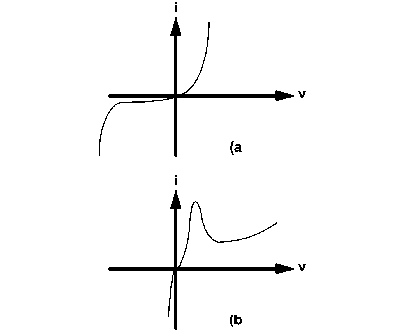 |
4.1 The v-i characteristics of (a) an ordinary pn-junction diode and (b) a tunnel diode. |
IPWLR -Type Model
The IPWLR model type is reserved for piecewise-linear v-i characteristics which are current-defined in the sense that the value of voltage is uniquely defined for every value of current. In such a case, the voltage-current coordinates at the points of definition of the v-i characteristics must satisfy the following restrictions:
- Values of the currents must be entered in a strictly ascending order: ???MATH???y0 < y1 < y2 ... < yk ???MATH???
- The slopes of the first and last segments must be positive: ???MATH???x0 < x1???MATH??? and ???MATH???xk -1 < xk???MATH???
For example, the v-i characteristics of the ordinary pn-junction diode shown in diagram 4.1(a) above and the v-i characteristics shown in diagram 4.2 can both be considered to behave as nonlinear current-defined resistors. Therefore, each can be approximated by an IPWLR-type model. On the other hand, the tunnel diode characteristics shown in diagram 4.1(b) cannot be modeled by an IPWLR-type model since the values for the branch voltage are not uniquely defined for every value of current. Similarly, the v-i characteristics shown in 4.2 cannot be modeled by a VPLWR-type model.
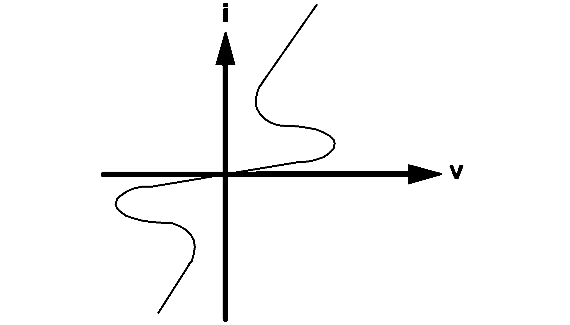 |
4.2 Example of a type of v-i characteristics that can be described as a current-defined resistor. |
Piecewise-Linear Inductor and Capacitor Models
The model statements for piecewise-linear inductors and capacitors are very similar to those for the piecewise-linear resistors. In the case of a piecewise-linear resistor, its characteristics are defined in terms of points on the current vs voltage plane. In the case of a piecewise-linear inductor, the characteristics are defined in terms of points on the flux-linkage vs. current plane. In the case of a piecewise-linear capacitor, the characteristics are defined in terms of points on the charge vs voltage plane.
The model statement format for a piecewise-linear inductor or capacitor is:
.MODEL  mname  mtype  NSEG=k  X0=x0  Y0=y0
+ X1=x1  Y1=y1  X2=x2  Y2=y2 ...  Xk=xk  Yk=yk
where
| .MODEL | is the six-character keyword ".MODEL" |
| mname | is a legal model name as explained in Model Names andSubcircuit Names |
| mtype | is a four-character keyword equal to "PWLL" or "PWLC", which stand for the model types for a piecewise-linear inductor or capacitor, respectively |
| NSEG= | is the five-character keyword "NSEG=" representing the number of linear segments in this device model |
| k | is an integer defining the number of linear segments and can take on values from 2 to 255, inclusively |
| X0= | is the keyword "X0=" representing the x axis coordinate of the beginning of the first linear segment of the device model |
| x0 | is a floating-point number which defines the value of X0 and has units of amperes for a PWL inductor and volts for a PWL capacitor. |
| Y0= | is the keyword "Y0=" representing the y axis coordinate of the beginning of the first linear segment of the device model |
| y0 | is a floating-point number which defines the value of Y0 and has units of weber-turns for a PWL inductor and coulombs for a PWL capacitor |
| X1= | is the keyword "X1=" representing the x axis coordinate of the end of the first linear segment of the device model and the beginning of the second linear segment of the device model |
| x1 | is a floating-point number which defines the value of X1 and has the same units indicated for x0 |
| Y1= | is the keyword "Y1=" representing the y axis coordinate of the end of the first linear segment of the device model and the beginning of the second linear segment of the device model, so that the straight line passing through (x0, y0) and terminating on the break point (x1, y1) forms the first segment of the piecewise-linear characteristic |
| y1 | is a floating-point number which defines the value of Y1 |
| X2= | is the keyword "X2=" representing the x axis coordinate of the end of the second linear segment of the device model and the beginning of the third linear segment of the device model |
| x2 | is a floating-point number which defines the value of X2. |
| Y2= | is the keyword "Y2=" representing the y axis coordinate of the end of the second linear segment of the device model and the beginning of the third linear segment of the device model, so that the straight line passing through (x1, y1) and terminating on the break point (x2, y2) forms the second segment of the piecewise-linear characteristic |
| y2 | is a floating-point number which defines the value of Y2, and so on |
| Xk= | is the keyword "Xk=" representing the x axis coordinate of the end of the last linear segment of the device model |
| xk | is a floating-point number which defines the value of Xk. |
| Yk= | is the keyword "Yk=" representing the y axis coordinate of the end of the last linear segment of the device model, so that the straight line starting at the break point (???MATH???xk-1???MATH???, ???MATH???yk-1???MATH???) and passing through the point (xk, yk) forms the last segment of the piecewise-linear characteristic, and |
| yk | is a floating-point number which defines the value of Yk. |
\[ x0 < x1 < x2 < ... < xk \]
\[ y0 < y1 < y2 < ... < yk \]
Simple Switch Models
SIMPLIS accepts two types of simple switch models:
- model type VCSW for a voltage-controlled switch, and
- model type ICSW for a current-controlled switch.
.MODEL  mname  mtype  RON=ron  ROFF=roff
+ TH=threshold  HYSTWD=hystwd  LOGIC={POS|NEG}
where
| .MODEL | is the six-character keyword ".MODEL" |
| mname | is a legal model name as explained in Model Names and Subcircuit Names |
| mtype | is a four-character keyword equal to either "VCSW" or "ICSW", indicating whether the switch is voltage-controlled or current-controlled |
| RON= | is the four-character keyword "RON=" representing the resistance in ohms of the switch when it is in the closed, or on, state |
| ron | is a positive floating-point number which defines the resistance in ohms of the switch when it is in the closed, or on, state |
| ROFF= | is the five-character keyword "ROFF=" representing the leakage resistance in ohms of the switch when it is in the open state |
| roff | is a positive floating-point number which defines the leakage resistance of the switch in ohms when it is at the open state |
| TH= | is the three-character keyword "TH=" representing the threshold value of the controlling signal. Together with HYSTWD, it determines the values at which the state of the switch will be changed from an open state to a closed state and vice versa |
| threshold | is a floating-point number which defines the threshold value of the controlling signal and is measured in volts for a voltage-controlled switch and measured in amperes for a current-controlled switch |
| HYSTWD= | is the seven-character keyword "HYSTWD=" representing the hysteresis width of the controlling signal |
| hystwd | is a positive floating-point number which defines the hysteresis width of the controlling signal and has the same unit of measurement as that of threshold. |
| LOGIC= | is the six-character keyword "LOGIC=" |
| POS | is the three-character string "POS" |
| NEG | is the three-character string "NEG". |
The diagram below defines the state of the simple switch, under two operating modes. If LOGIC is assigned the value POS, the switching of the simple switch is defined by (a). If LOGIC is assigned the value NEG, the switching logic is reversed, and the state of the simple switch is then defined by (b).
When a simple switch is in the closed state, it is modeled by a linear resistor having a resistance equal to ron between its positive node and negative node. When the simple switch is in the open state, the resistance of the linear resistor changes to roff.
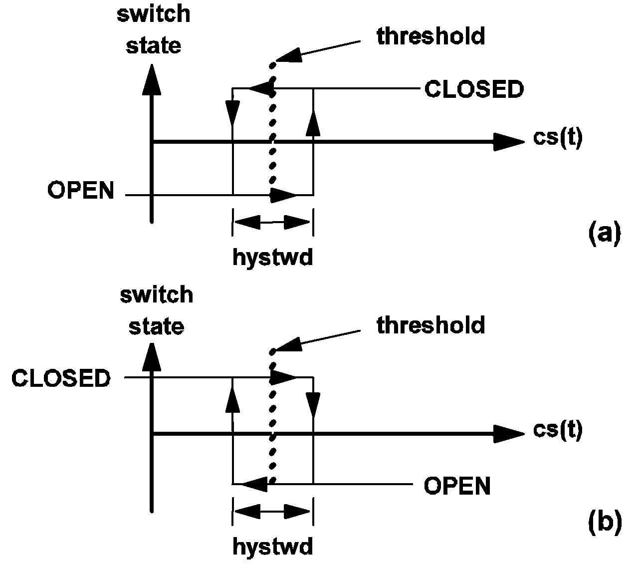 |
4.3 State diagram of the simple switch when the parameter LOGIC is assigned a value of (a) POS or (b) NEG. |
Simple Transistor Switch Models
There are four simple transistor models, composed of:
- a set of two voltage-controlled models, designated as VCQPOS and VCQNEG;
- a set of two current-controlled models, designated as ICQPOS and ICQNEG.
.MODEL  mname  mtype  VSAT=vsat  RSAT=rsat
+ ROFF=roff  GAIN=gain  TH=threshold
+ HYSTWD=hystwd  LOGIC={POS|NEG}  LEVEL={1|2}
where
| .MODEL | is the six-character keyword ".MODEL" |
| mname | is a legal model name as explained in Model Names and Subcircuit Names |
| mtype | is a six-character keyword equal to one of the following keywords: "VCQPOS", "VCQNEG", "ICQPOS", and "ICQNEG" |
| VSAT= | is the five-character keyword "VSAT=" |
| vsat | is a floating-point number which defines the saturation voltage of the transistor switch in volts. It is the voltage across the transistor switch when it is saturated and the current through it is negligibly small. It is a positive number for VCQPOS-type and ICQPOS-type transistor switches and it is a negative number for VCQNEG-type and ICQNEG-type transistor switches, |
| RSAT= | is the five-character keyword "RSAT=" |
| rsat | is a positive number which defines the saturation resistance in ohms of the transistor switch |
| ROFF= | is the five-character keyword "ROFF=" |
| roff | is a positive number which defines the leakage resistance of the switch in ohms when it is at the open state. It must be larger than rsat |
| GAIN= | is the five-character keyword "GAIN=" |
| gain | is a positive floating-point number which defines the gain of the transistor switch when the parameter LEVEL is assigned a value above 1. Its value is ignored when LEVEL is assigned a value of 1 |
| TH= | is the three-character keyword "TH=" |
| threshold | is a floating-point number which defines the threshold value of the controlling signal. Together with hystwd, it determines the values at which the transistor switch will be changed from an OPEN state to a CLOSE state and vice versa. It is measured in volts for VCQPOS- and VCQNEG-type switches and measured in amperes for ICQPOS- and ICQNEG-type switches |
| HYSTWD= | is the seven-character keyword "HYSTWD=" |
| hystwd | is a positive floating-point number which defines the hysteresis width of the controlling signal. It has the same unit of measurement as that of threshold |
| LOGIC= | is the six-character keyword "LOGIC=" |
| POS | is the three-character keyword "POS" |
| NEG | is the three-character keyword "NEG", |
| LEVEL= | is the six-character keyword "LEVEL=" |
| 1 | is the integer 1 |
| 2 | is the integer 2 |
For model types VCQPOS and ICQPOS, the voltage across the transistor switch, measured as the voltage of the positive node with respect to the voltage of the negative node, assumes nonnegative values under normal operation like an NPN bipolar transistor and an N-channel MOSFET. For model types VCQNEG and ICQNEG, the voltage across the transistor switch, measured as the voltage of the positive node with respect to the voltage of the negative node, assumes non positive values under normal operation like a PNP bipolar transistor and a P-channel MOSFET.
Models for Simple Transistor Switches for LEVEL=1
When a simple transistor switch is modeled with the LEVEL parameter set to 1, it can assume either an open or a closed state. The switching diagram in 4.3 (a) applies when LOGIC is set to POS while the switching diagram in 4.3 (b) applies when LOGIC is set to NEG.
The only difference between a simple switch and a simple transistor switch with LEVEL set to 1 is the model of the closed state. When a simple transistor switch with LEVEL set to 1 is in the closed state, it is modeled by a linear resistor with the value rsat in series with a constant voltage source with the value vsat. When the simple transistor switch is in the open state, it is modeled by a resistor with the value roff. The block diagram and the V-I characteristic of the model are shown in Figure 4.4. The circuit element model of the simple transistor switch with LEVEL set to 1 for the closed and open states are shown in diagram 4.4 below.
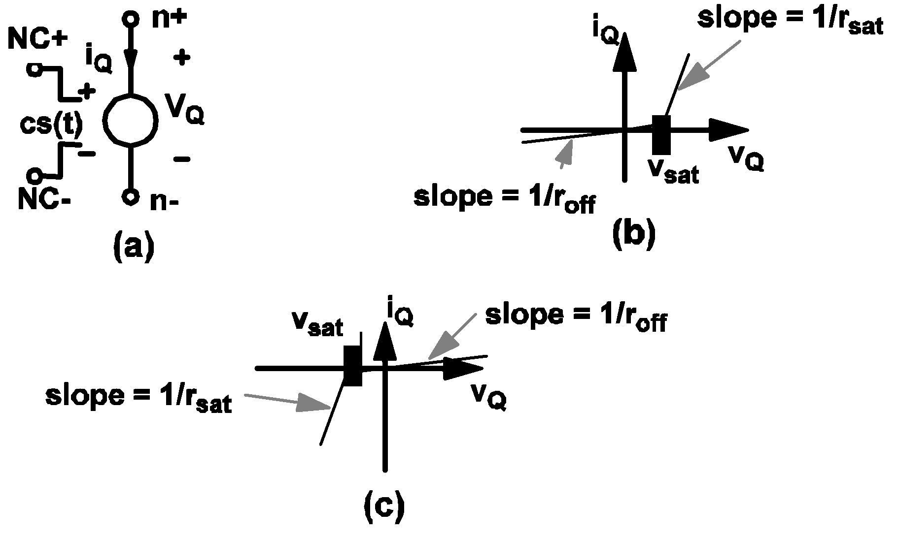 |
4.4 Model for the simple transistor switch: (a) Simple transistor switch controlled by a control signal cs(t), (b) the i Q vs v Q characteristic of the simple POS-type transistor switch, and (c) the i Q vs v Q characteristic of the simple NEG-type transistor switch. |
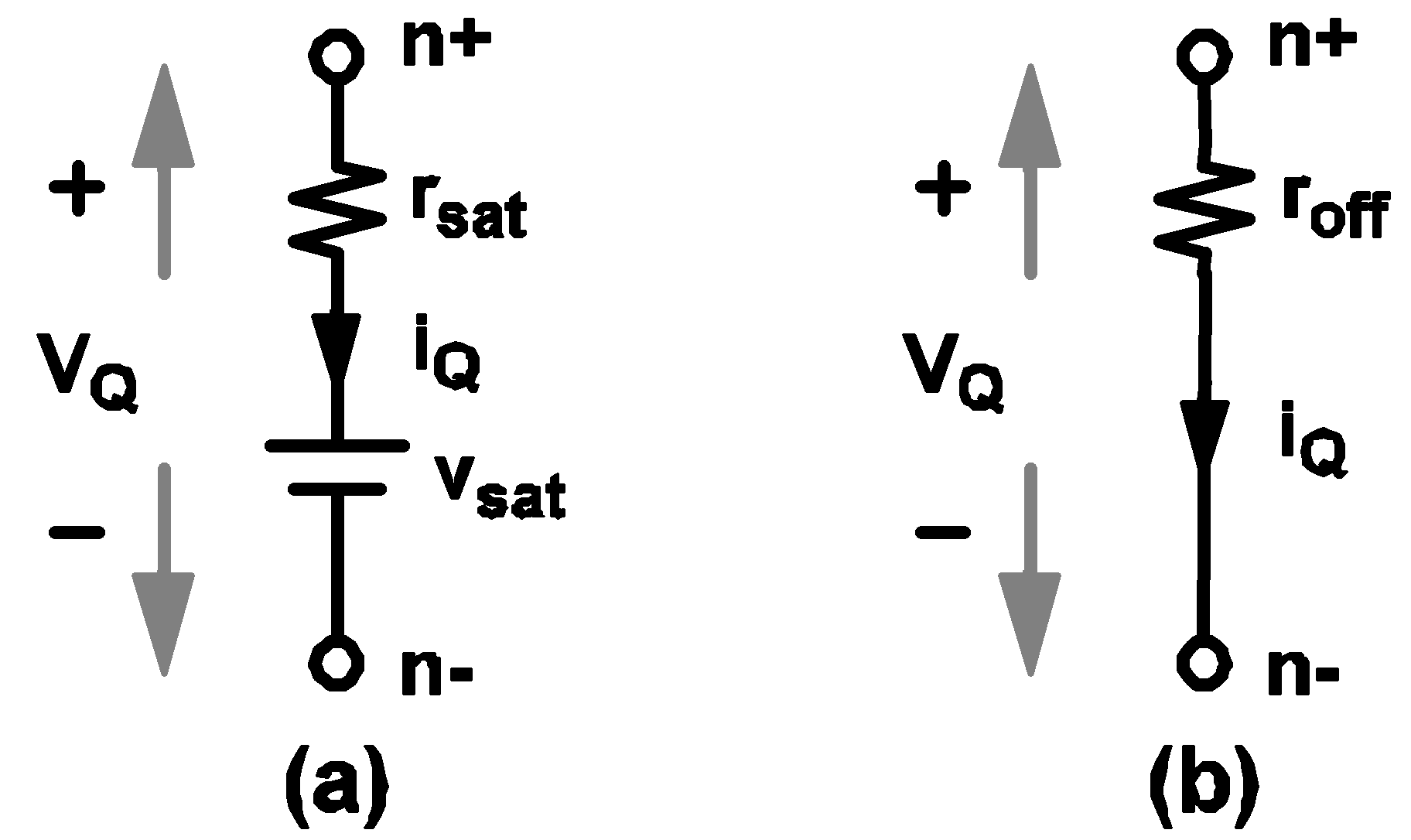 |
4.5 Model for the simple transistor switch: (a) model of the simple transistor switch for LEVEL=1 when it is in a closed state, and (b) model of the simple transistor switch for LEVEL=1 when it is in an open state. |
If a physical transistor is being driven to act like a switch and detailed waveforms of the voltage across the transistor and the current through the transistor are not critically important, it is recommended that such a transistor be modeled by a simple transistor switch with the parameter LEVEL set to 1 since the simulation is faster when a transistor switch has LEVEL set to 1.
When a simple transistor switch is modeled with the LEVEL parameter set to 1, the value of the GAIN parameter has no effect on the modeling. In addition, the direction of current flow through the transistor switch is not restricted and the device behaves more like a controlled switch than a physical transistor.
Models for Simple Transistor Switches for LEVEL=2
When a simple transistor switch is modeled with the LEVEL parameter set to 2, it still assumes either an open state or a closed state. The switching diagram in 4.3(a) still applies when LOGIC is set to POS while the switching diagram in 4.3 (b) still applies when LOGIC is set to NEG.
When the LEVEL parameter is set to 2, the simple transistor is still modeled by a resistor with a resistance equal to roff when it is in the open state. When the simple transistor switch is in the closed state, additional secondary states are provided for the simple transistor, allowing the modeling of a physical transistor at operating areas where both the voltage across and the current through the transistor are simultaneously substantial. For bipolar transistors, such operating areas are collectively called the active region. For the simple transistor switch the individual states are called ACTIVE, SATURATE, and REV_BIASED, to stand for active region, saturation, and reversed-biased, as indicated in 4.6 . SIMPLIS internally computes the voltage across and the current through the simple transistor switch to determine the correct secondary state at which the transistor switch should operate.
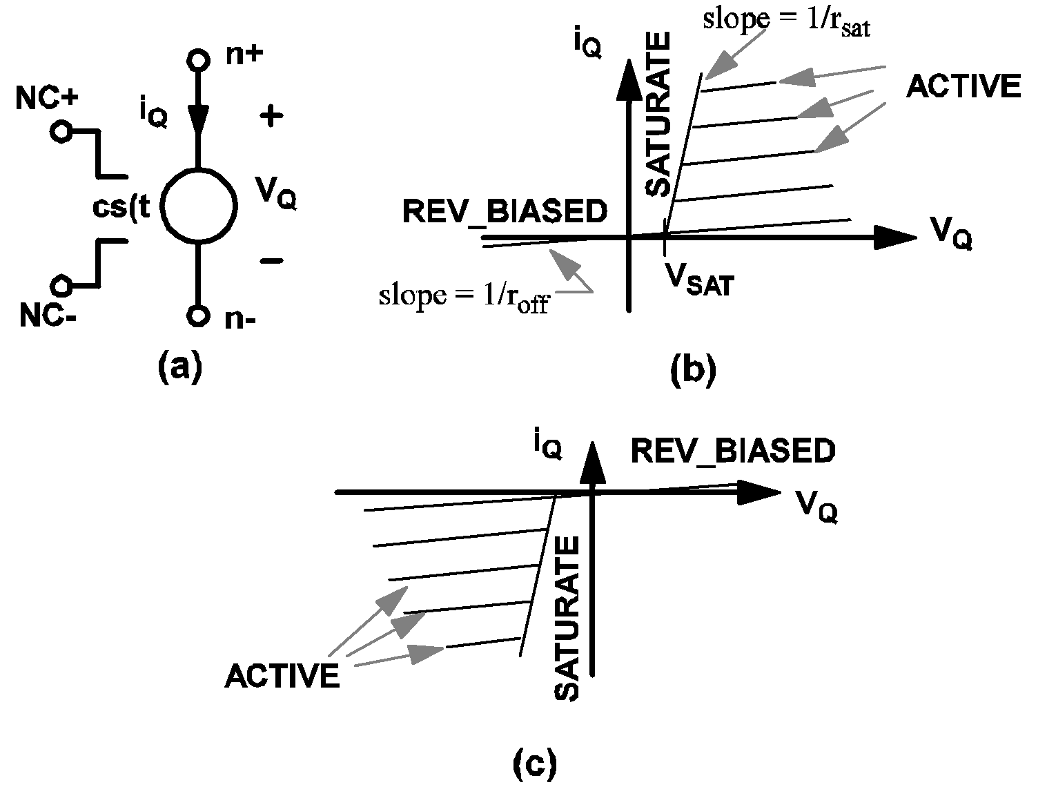 |
4.6 Model for the simple transistor switch for LEVEL=2. (a) A simple transistor switch controlled by a control signal cs(t), (b) The i Q vs v Q characteristics of a VCQPOS-type or ICQPOS-type transistor switch, (c) The i Q vs v Q characteristic of a VCQNEG-type or ICQNEG-type transistor switch. |
When the secondary state of a simple transistor switch is equal to ACTIVE, it is modeled by a parallel combination of a linear resistor with a resistance equal to roff and a controlled-current source ci(t) as indicated in 4.7(a). The current ci(t) of the controlled-current source is defined by the following equations if LOGIC is set to POS:
ci(t) = gain * [cs(t) - (threshold - hystwd/2)]
for  VCQPOS-type transistor switches and
for  ICQPOS-type transistor switches
AND
ci(t) = - gain * [ cs(t) - (threshold - hystwd/2) ]
for  VCQNEG-type transistor switches and
for  ICQNEG-type transistor switches.
On the other hand, the current ci(t) of the controlled-current source is defined by the following equations if LOGIC is set to NEG:
ci(t) = - gain * [ cs(t) - (threshold + hystwd/2) ]
for  VCQPOS-type transistor switches and
for  ICQPOS-type transistor switches, and
AND
ci(t) = gain * [ cs(t) - (threshold + hystwd/2) ]
for  VCQNEG-type transistor switches and
for  ICQNEG-type transistor switches.
For example, an NPN transistor can be modeled by a piecewise-linear resistor to represent the base-emitter characteristics and an ICQPOS-type simple transistor switch with LEVEL and LOGIC set to 2 and POS, respectively, to represent the collector-emitter characteristics. Similarly, the collector-emitter characteristics of a PNP transistor can be modeled by an ICQNEG-type transistor switch with LEVEL and LOGIC set to 2 and NEG, respectively.
When the secondary state of a simple transistor switch is equal to SATURATE, it is modeled by the small network as shown in 4.7(b), which comprises a linear resistor with a resistance equal to rsat in series with a voltage source with source value vsat. When the secondary state of a simple transistor switch is equal to REV_BIASED, it is modeled by a large resistor with resistance equal to roff as shown in 4.7 (c).
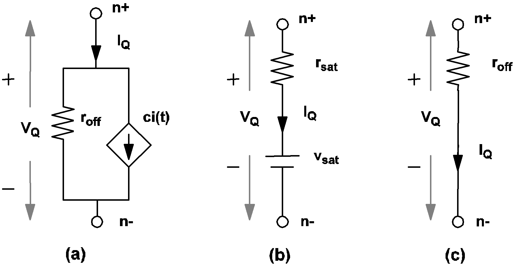 |
4.7 Model of a simple transistor switch in the closed state, with LEVEL=2. (a) Model for the ACTIVE secondary state, (b) Model for the SATURATE secondary state, (c) Model for the REV_BIASED secondary state. |
By selecting LEVEL=2 in the simple transistor switch model, you can more accurately model a physical transistor and are able to obtain more detailed waveforms on the voltage and current for the device. The penalty is an increase in the simulation time since more variables need to be monitored and computed throughout the simulation.
Simple Logic Device Models
To aid the understanding of the models for simple logic devices, the concept of "positive" and "negative" logic is discussed first. Except for inverters and comparators, all logic gates use a parameter called LOGIC in the model statement. The purpose of this parameter is to define whether a "positive logic" or a "negative logic" convention is used in defining the logic states.
If the LOGIC parameter is set to POS, positive logic is used to determine the logic states of the inputs and the output. This means a state of logic 0 is represented by a lower voltage level than that of a state of logic 1. In this case, the input logic state of an input node is defined to be at logic 1 if
V(ni,nref) >= threshold + hystwd/2where ni and nref are the node names of the input node and reference node, respectively.
The input logic state is considered to be at logic 0 if
V(ni,nref) <= threshold - hystwd/2The output logic state is equal to the result of the boolean operator associated with the gate applied to the input logic states. If the output state is equal to logic 1, the value of the voltage source in the output circuit is set to voh. If the output state is equal to logic 0, the value of the voltage source in the output circuit is set to vol. The two parameters vol and voh are specified in the model statement.
If the LOGIC parameter is set to NEG, negative logic is used to determine the logic states of the inputs and the output. Negative logic means a state of logic 0 is represented by a higher voltage level than that of a state of logic 1. In this case, the input logic state of an input node ni is defined to be at logic 1 if
V(ni,nref) <= threshold - hystwd/2and it is considered to be at logic 0 if
V(ni,nref) >= threshold + hystwd/2The output logic state is equal to the result of the boolean operator associated with the gate applied to the input logic states. If the output state is equal to logic 1, the value of the voltage source, vout, in the output circuit is set to vol. If the output state is equal to logic 0, the value of vout is set to voh.
Inverter Model
The format for the inverter model statement is:
.MODEL  mname  INV  TH=threshold  HYSTWD=hystwd
+ VOL=vol  VOH=voh  RIN=rin  ROUT=rout
where
| .MODEL | is the six-character keyword ".MODEL", |
| mname | is a legal model name as explained in Model Names and Subcircuit Names |
| INV | is the three-character keyword "INV" which identifies the inverter-type simple logic gates |
| TH= | is the three-character keyword "TH=" |
| threshold | is a floating-point number which defines the threshold value of the input voltage in volts. Together with hystwd, it determines the values of the input voltage at which the output states of the inverter will be changed from a logic 0 to a logic 1 and vice versa |
| HYSTWD= | is the seven-character keyword "HYSTWD=" |
| hystwd | is a positive floating-point number to represent the hysteresis width of the input voltage in volts |
| VOL= | is the four-character keyword "VOL=" |
| vol | is a floating-point number which defines the low value of the output voltage in volts |
| VOH= | is the four-character keyword "VOH=" |
| voh | is a floating-point number which defines the high value of the output voltage in volts. It must be larger than vol |
| RIN= | is the four-character keyword "RIN=" |
| rin | is a floating-point number which defines the input resistance in ohms |
| ROUT= | is the five-character keyword "ROUT=" |
| rout | is a floating-point number which defines the output resistance in ohms. |
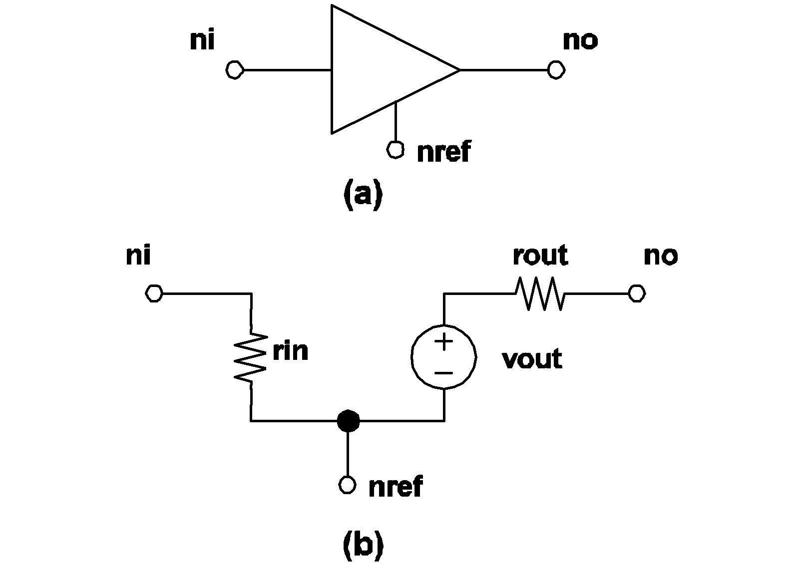 |
4.8 SIMPLIS inverter model: (a) Symbol for inverter, (b) Model for inverter. The nodes ni, no and nref are the input, output and the reference nodes, respectively. |
If the output state of an inverter is equal to logic 1, the value of the voltage source, vout, in the output circuit is set to voh. In this case, the output state of the device is changed to logic 0 when
V(ni,nref) >= threshold + hystwd/2where V(ni,nref) represents the voltage of the input node with respect to the reference node.
If the output state of an inverter is equal to logic 0, the value of the voltage source, vout, in the output circuit is set to vol. In this case, the output state of the device is changed to logic 1 when
V(ni,nref) <= threshold - hystwd/2
Comparator Model
The format for the comparator model statement is:
s.MODEL  mname  COMP HYSTWD=hystwd  VOL=vol  VOH=voh
+ RIN=rin  ROUT=rout
where
| .MODEL | is the six-character keyword ".MODEL" |
| mname | is a legal model name as explained in Model Names and Subcircuit Names |
| COMP | is the four-character keyword "COMP" to stand for comparator-type simple logic gates |
| HYSTWD= | is the seven-character keyword "HYSTWD=" |
| hystwd | is a positive floating-point number which defines the hysteresis width of the differential input voltage in volts |
| VOL= | is the four-character keyword "VOL=" |
| vol | is a floating-point number which defines the low value of the output voltage in volts |
| VOH= | is the four-character keyword "VOH=" |
| voh | is a floating-point number which defines the high value of the output voltage in volts. It must be larger than vol |
| RIN= | is the four-character keyword "RIN=" |
| rin | is a floating-point number which defines the input resistance in ohms |
| ROUT= | is the five-character keyword "ROUT=" |
| rout | is a floating-point number which defines the output resistance in ohms. |
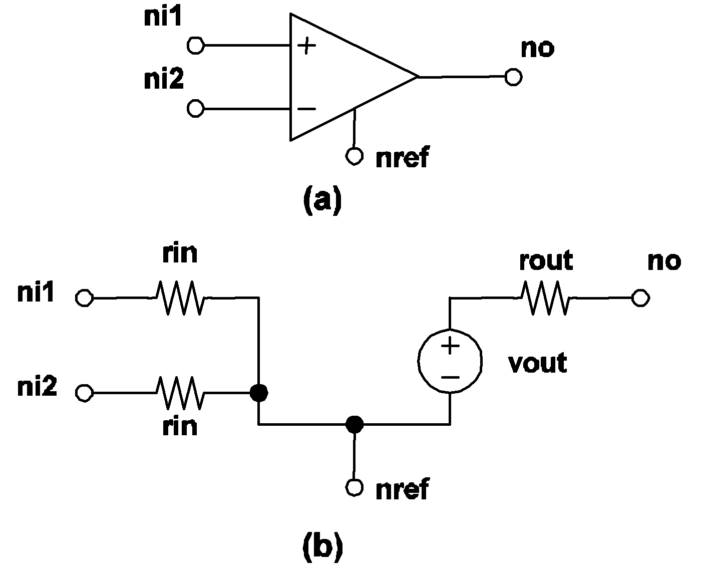 |
4.9 SIMPLIS comparator model: (a) Symbol for comparator, (b) Model for comparator. The nodes n1, n2 are the two input nodes. The nodes no and nref are the output and reference nodes, respectively. |
If the output state of a comparator is equal to logic 1, the value of the voltage source, vout, in the output circuit is set to voh. In this case, the output state of the device is changed to logic 0 when
V(ni1,ni2) <= - hystwd/2where V(ni1,ni2) represents the voltage of the first input node with respect to the voltage of the second input node.
If the output state of a comparator is equal to logic 0, the value of the voltage source, vout, in the output circuit is set to vol. In this case, the output state of the device is changed to logic 1 when
V(ni1,ni2) >= hystwd/2
Exclusive-OR Gate Model
The format for the Exclusive-OR model statement is:
.MODEL  mname  XOR TH=threshold  HYSTWD=hystwd
+ VOL=vol  VOH=voh  RIN=rin  ROUT=rout
+ LOGIC={POS | NEG}
where
| .MODEL | is the six-character keyword ".MODEL" |
| mname | is a legal model name as explained in Model Names and Subcircuit Names |
| XOR | is the three-character keyword "XOR" to stand for exclusive-OR type simple logic gates |
| TH= | is the three-character keyword "TH=" |
| threshold | is a floating-point number which defines the threshold value of the input voltage in volts. Together with hystwd, it determines the values of the input voltage at which the input states of the exclusive-OR gate will be changed from a logic 0 to a logic 1 and vice versa |
| HYSTWD= | is the seven-character keyword "HYSTWD=" |
| hystwd | is a positive floating-point number which defines the hysteresis width of the input voltage in volts |
| VOL= | is the four-character keyword "VOL=" |
| vol | is a floating-point number representing the low value of the output voltage in volts |
| VOH= | is the four-character keyword "VOH=" |
| voh | is a floating-point number which defines the high value of the output voltage in volts. It must be larger than the value of vol |
| RIN= | is the four-character keyword "RIN=" |
| rin | is a floating-point number which defines the input resistance in ohms |
| ROUT= | is the five-character keyword "ROUT=" |
| rout | is a floating-point number which defines the output resistance in ohms |
| LOGIC= | is the six-character keyword "LOGIC=" |
| POS | is the three-character keyword "POS" |
| NEG | is the three-character keyword "NEG" |
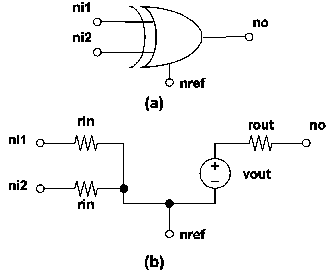 |
4.10 Exclusive-OR gate model: (a) Symbol for exclusive-OR gate, (b) Model for exclusive-OR gate. The nodes ni1 and ni2 are the two input nodes. The nodes no and nref are the output and reference nodes, respectively. |
The actual model implemented in SIMPLIS for an exclusive-OR gate is shown in 4.10 (a). The source value of the voltage source, vout, in the output circuit depends on the logic state of the output of the gate. The output state is equal to the result of the boolean EXCLUSIVE-OR operation on the two input states.
OR Gate Model
The format for the OR Gate model statement is:
.MODEL mname  ORk TH=threshold  HYSTWD=hystwd
+ VOL=vol  VOH=voh  RIN=rin  ROUT=rout
+ LOGIC={POS | NEG}
where
| .MODEL | is the six-character keyword ".MODEL" |
| mname | is a legal model name as explained in Model Names and Subcircuit Names |
| OR | is the two-character keyword "OR" to stand for OR-type simple logic gates |
| k | is an integer from 2 to 9, inclusively, which defines the number of inputs for the OR gate |
| TH= | is the three-character keyword "TH=" |
| threshold | is a floating-point number which defines the threshold value of the input voltage in volts, and together with hystwd, it determines the values of the input voltage at which the input states of the exclusive-OR gate will be changed from a logic 0 to a logic 1 and vice versa |
| HYSTWD= | is the seven-character keyword "HYSTWD=" |
| hystwd | is a positive floating-point number which defines the hysteresis width of the input voltage in volts |
| VOL= | is the four-character keyword "VOL=" |
| vol | is a floating-point number representing the low value of the output voltage in volts |
| VOH= | is the four-character keyword "VOH=" |
| voh | is a floating-point number which defines the high value of the output voltage in volts. It must be larger than the value of vol |
| RIN= | is the four-character keyword "RIN=" |
| rin | is a floating-point number which defines the input resistance |
| ROUT= | is the five-character keyword "ROUT=" |
| rout | is a floating-point number which defines the output resistance in ohms |
| LOGIC= | is the six-character keyword "LOGIC=" |
| POS | is the three-character keyword "POS" |
| NEG | is the three-character keyword "NEG" |
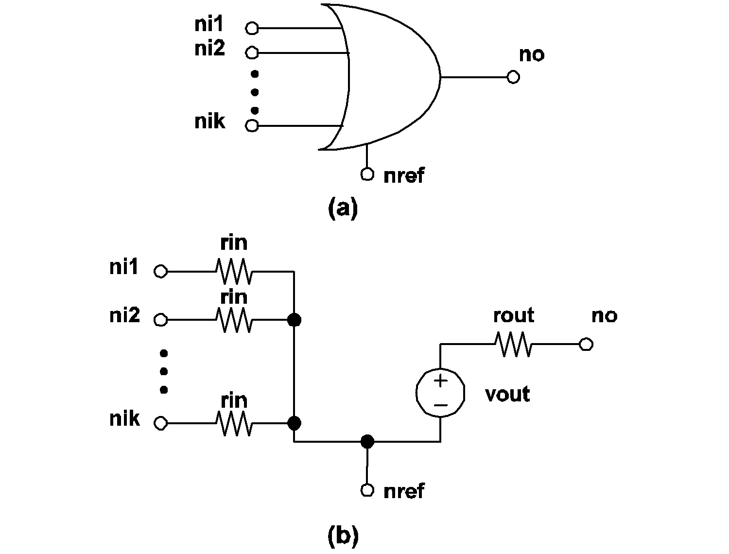 |
4.11 k-Input OR gate model: (a) Symbol for k-Input OR gate, (b) Model for k-Input OR gate. The nodes ni1 and ni2 are the two input nodes. Up to a maximum of 9 inputs can be accommodated. |
The actual model implemented in SIMPLIS for a k-input OR gate is shown in 4.11 (b). The output state is equal to the result of the boolean OR operation applied to the k input states.
NOR Gate Model
The format for the NOR Gate model statement is:
.MODEL mname NORk TH=threshold  HYSTWD=hystwd
+ VOL=vol  VOH=voh  RIN=rin  ROUT=rout
+ LOGIC={POS | NEG}
where
| .MODEL | is the six-character keyword ".MODEL" |
| mname | is a legal model name as explained in Model Names and Subcircuit Names |
| NOR | is the three-character keyword "NOR" to stand for NOR-type simple logic gates |
| k | is an integer from 2 to 9, inclusively, indicating the number of inputs for the NOR gate |
| TH= | is the three-character keyword "TH=" |
| threshold | is a floating-point number which defines the threshold value of the input voltage in volts, and together with hystwd, it determines the values of the input voltage at which the input states of the exclusive-OR gate will be changed from a logic 0 to a logic 1 and vice versa |
| HYSTWD= | is the seven-character keyword "HYSTWD=" |
| hystwd | is a positive floating-point number which defines the hysteresis width of the input voltage in volts |
| VOL= | is the four-character keyword "VOL=" |
| vol | is a floating-point number representing the low value of the output voltage in volts |
| VOH= | is the four-character keyword "VOH=" |
| voh | is a floating-point number which defines the high value of the output voltage in volts and must be larger than vol |
| RIN= | is the four-character keyword "RIN=" |
| rin | is a floating-point number which defines the input resistance |
| ROUT= | is the five-character keyword "ROUT=" |
| rout | is a floating-point number which defines the output resistance in ohms |
| LOGIC= | is the six-character keyword "LOGIC=" |
| POS | is the three-character keyword "POS" |
| NEG | is the three-character keyword "NEG" |
AND Gate Model
The format for the AND Gate model statement is:
.MODEL mname ANDk TH=threshold  HYSTWD=hystwd
+ VOL=vol  VOH=voh  RIN=rin  ROUT=rout
+ LOGIC={POS | NEG}
where
| .MODEL | is the six-character keyword ".MODEL" |
| mname | is a legal model name as explained in Model Names and Subcircuit Names |
| AND | is the three-character keyword "AND" to stand for AND-type simple logic gates |
| k | is an integer from 2 to 9, inclusively, to stand for the number of inputs for the AND gate |
| TH= | is the three-character keyword "TH=" |
| threshold | is a floating-point number which defines the threshold value of the input voltage in volts, which together with hystwd, determines the values of the input voltage at which the input states of the exclusive-OR gate will be changed from a logic 0 to a logic 1 and vice versa |
| HYSTWD= | is the seven-character keyword "HYSTWD=" |
| hystwd | is a positive floating-point number which defines the hysteresis width of the input voltage in volts |
| VOL= | is the four-character keyword "VOL=" |
| vol | is a floating-point number representing the low value of the output voltage in volts |
| VOH= | is the four-character keyword "VOH=" |
| voh | is a floating-point number which defines the high value of the output voltage in volts and must be larger than vol |
| RIN= | is the four-character keyword "RIN=" |
| rin | is a floating-point number which defines the input resistance |
| ROUT= | is the five-character keyword "ROUT=" |
| rout | is a floating-point number which defines the output resistance in ohms |
| LOGIC= | is the six-character keyword "LOGIC=" |
| POS | is the three-character keyword "POS" |
| NEG | is the three-character keyword "NEG" |
NAND Gate Model
The format for the NAND gate model statement is:
.MODEL mname NANDk TH=threshold  HYSTWD=hystwd
+ VOL=vol  VOH=voh  RIN=rin  ROUT=rout
+ LOGIC={POS | NEG}
where
| .MODEL | is the six-character keyword ".MODEL" |
| mname | is a legal model name as explained in Model Names and Subcircuit Names |
| NAND | is the four-character keyword "NAND" to stand for NAND-type simple logic gates |
| k | is an integer from 2 to 9, inclusively, to stand for the number of inputs for the NAND gate |
| TH= | is the three-character keyword "TH=" |
| threshold | is a floating-point number which defines the threshold value of the input voltage in volts, which together with hystwd, determines the values of the input voltage at which the input states of the exclusive-OR gate will be changed from a logic 0 to a logic 1 and vice versa |
| HYSTWD= | is the seven-character keyword "HYSTWD=" |
| hystwd | is a positive floating-point number which defines the hysteresis width of the input voltage in volts |
| VOL= | is the four-character keyword "VOL=" |
| vol | is a floating-point number representing the low value of the output voltage in volts |
| VOH= | is the four-character keyword "VOH=" |
| voh | is a floating-point number which defines the high value of the output voltage in volts and must be larger than vol |
| RIN= | is the four-character keyword "RIN=" |
| rin | is a floating-point number which defines the input resistance |
| ROUT= | is the five-character keyword "ROUT=" |
| rout | is a floating-point number which defines the output resistance in ohms |
| LOGIC= | is the six-character keyword "LOGIC=" |
| POS | is the three-character keyword "POS" |
| NEG | is the three-character keyword "NEG" |
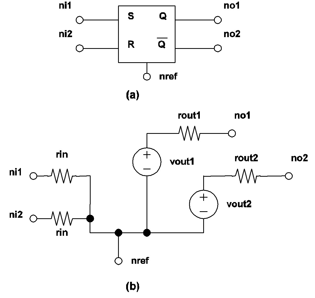
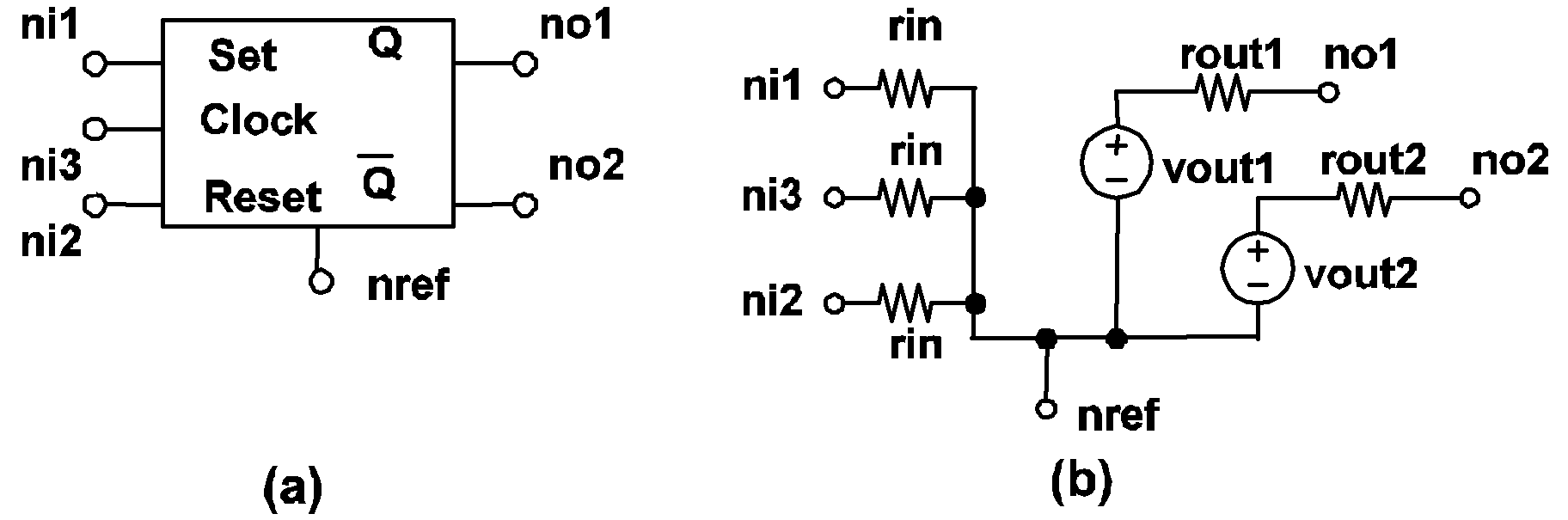
Set-Reset Flip Flop Model
The format for the Set-Reset flip flop model statement is:
.MODEL mname SRFF TH=threshold  HYSTWD=hystwd
+ VOL=vol  VOH=voh  RIN=rin  ROUT=rout
+ LOGIC={POS | NEG}
where
| .MODEL | is the six-character keyword ".MODEL" |
| mname | is a legal model name as explained in Model Names and Subcircuit Names |
| SRFF | is the four-character keyword "SRFF" to stand for SRFF-type simple logic gates |
| TH= | is the three-character keyword "TH=" |
| threshold | is a floating-point number which defines the threshold value of the input voltage in volts, which together with hystwd, determines the values of the input voltage at which the input states of the exclusive-OR gate will be changed from a logic 0 to a logic 1 and vice versa |
| HYSTWD= | is the seven-character keyword "HYSTWD=" |
| hystwd | is a positive floating-point number which defines the hysteresis width of the input voltage in volts |
| VOL= | is the four-character keyword "VOL=" |
| vol | is a floating-point number representing the low value of the output voltage in volts |
| VOH= | is the four-character keyword "VOH=" |
| voh | is a floating-point number which defines the high value of the output voltage in volts and must be larger than the value of vol |
| RIN= | is the four-character keyword "RIN=" |
| rin | is a floating-point number which defines the input resistance |
| ROUT= | is the five-character keyword "ROUT=" |
| rout | is a floating-point number which defines the output resistance in ohms |
| LOGIC= | is the six-character keyword "LOGIC=" |
| POS | is the three-character keyword "POS" |
| NEG | is the three-character keyword "NEG". |
The logic state of the output Q' is always equal to the logical complement of the logic state of the output Q. The initial condition specified in the device statement for an S-R flip-flop is used to initialize the logic output state of the normal output Q. When the logic state of the set input is equal to logic 1, the logic state of the normal output Q is set to logic 1. When the logic state of the reset input is equal to logic 1, the logic state of the normal output Q is set to logic 0.
The output state of an S-R flip flop is supposed to be undefined when the input logic states of the set and reset inputs are both equal to logic 1. For ease of debugging, the output state of the S-R flip-flop as implemented by SIMPLIS will remain unchanged when both input states are equal to logic 1. (See 4.12)
 |
4.12 SR Flip Flop model: (a) Symbol for a SIMPLIS S-R flip flop, (b) Model for a SIMPLIS S-R flip flop. |
Clocked Set-Reset Flip-Flop
.MODEL mname CLK_SRFF TH=threshold
+ HYSTWD=hystwd  VOL=vol  VOH=voh  RIN=rin
+ ROUT=rout  LOGIC={POS | NEG}
+ TRIG_COND={0_TO_1 | 1_TO_0}
where
| .MODEL | is the six-character keyword ".MODEL" |
| mname | is a legal model name as explained in Model Names and Subcircuit Names |
| CLK_SRFF | is the eight-character keyword "CLK_SRFF" to stand for CLK_SRFF-type simple logic gates |
| TH= | is the three-character keyword "TH=" |
| threshold | is a floating-point number which defines the threshold value of the input voltage in volts, which together with hystwd, determines the values of the input voltage at which the input states of the exclusive-OR gate will be changed from a logic 0 to a logic 1 and vice versa |
| HYSTWD= | is the seven-character keyword "HYSTWD=" |
| hystwd | is a positive floating-point number which defines the hysteresis width of the input voltage in volts |
| VOL= | is the four-character keyword "VOL=" |
| vol | is a floating-point number representing the low value of the output voltage in volts |
| VOH= | is the four-character keyword "VOH=" |
| voh | is a floating-point number which defines the high value of the output voltage in volts and must be larger than vol |
| RIN= | is the four-character keyword "RIN=" |
| rin | is a floating-point number which defines the input resistance |
| ROUT= | is the five-character keyword "ROUT=" |
| rout | is a floating-point number which defines the output resistance in ohms |
| LOGIC= | is the six-character keyword "LOGIC=" |
| POS | is the three-character keyword "POS" |
| NEG | is the three-character keyword "NEG". |
| TRIG_COND= | is the ten-character keyword "TRIG_COND=" |
| 0_TO_1 | is the six-character keyword "0_TO_1" |
| 1_TO_0 | is the six-character keyword "1_TO_0" |
If TRIG_COND = 0_TO_1, the clocked Set-Reset flip-flop is considered to be "triggered" when the logic state of the clock input changes from 0 to 1. Similarly, a logic 1 to logic 0 transition for the clock input is considered to "trigger" this type of flip-flop if TRIG_COND = 1_TO_0. The logic state of each output will not change except at the triggering moment. At the triggering moment, the logic of the clocked Set-Reset flip-flop is same as that of the unclocked Set-Reset flip-flop.
 |
4.13 Clocked SR Flip Flop model: (a) Symbol for a SIMPLIS Clocked S-R flip flop, (b) Model for a SIMPLIS Clocked S-R flip flop. |
Clocked J-K Flip-Flop
.MODEL mname CLK_JKFF TH=threshold
+ HYSTWD=hystwd  VOL=vol  VOH=voh  RIN=rin+ ROUT=rout  LOGIC={POS | NEG}
+ TRIG_COND={0_TO_1 | 1_TO_0}
| .MODEL | is the six-character keyword ".MODEL" |
| mname | is a legal model name as explained in Model Names and Subcircuit Names |
| CLK_JKFF | is the eight-character keyword "CLK_JKFF" to stand for CLK_JKFF-type simple logic gates |
| TH= | is the three-character keyword "TH=" |
| threshold | is a floating-point number which defines the threshold value of the input voltage in volts, which together with hystwd, determines the values of the input voltage at which the input states of the exclusive-OR gate will be changed from a logic 0 to a logic 1 and vice versa |
| HYSTWD= | is the seven-character keyword "HYSTWD=" |
| hystwd | is a positive floating-point number which defines the hysteresis width of the input voltage in volts |
| VOL= | is the four-character keyword "VOL=" |
| vol | is a floating-point number representing the low value of the output voltage in volts |
| VOH= | is the four-character keyword "VOH=" |
| voh | is a floating-point number which defines the high value of the output voltage in volts and must be larger than vol |
| RIN= | is the four-character keyword "RIN=" |
| rin | is a floating-point number which defines the input resistance |
| ROUT= | is the five-character keyword "ROUT=" |
| rout | is a floating-point number which defines the output resistance in ohms |
| LOGIC= | is the six-character keyword "LOGIC=" |
| POS | is the three-character keyword "POS" |
| NEG | is the three-character keyword "NEG" |
| TRIG_COND= | is the ten-character keyword "TRIG_COND=" |
| 0_TO_1 | is the six-character keyword "0_TO_1" |
| 1_TO_0 | is the six-character keyword "1_TO_0" |
If TRIG_COND = 0_TO_1, the clocked J-K flip-flop is considered to be "triggered" when the logic state of the clock input changes from 0 to 1. Similarly, a logic 1 to logic 0 transition for the clock input is considered to "trigger" this type of flip-flop if TRIG_COND = 1_TO_0. The logic state of each output will not change except at the triggering moment. At the triggering moment, the logic of the clocked J-K flip-flop is same as that of the unclocked Set-Reset flip-flop with one exception: if the states of both the J and the K inputs are equal to logic 1 at the triggering moment, the states of each output of a clocked J-K flip-flop will be set to the complement of its logic state right before the triggering moment. Hence, if the state of the normal output Q is equal to logic 1/0 right before the triggering moment, it will be set to logic 0/1 at the triggering moment if the states of both the J and the K inputs are equal to logic 1 at the triggering moment.
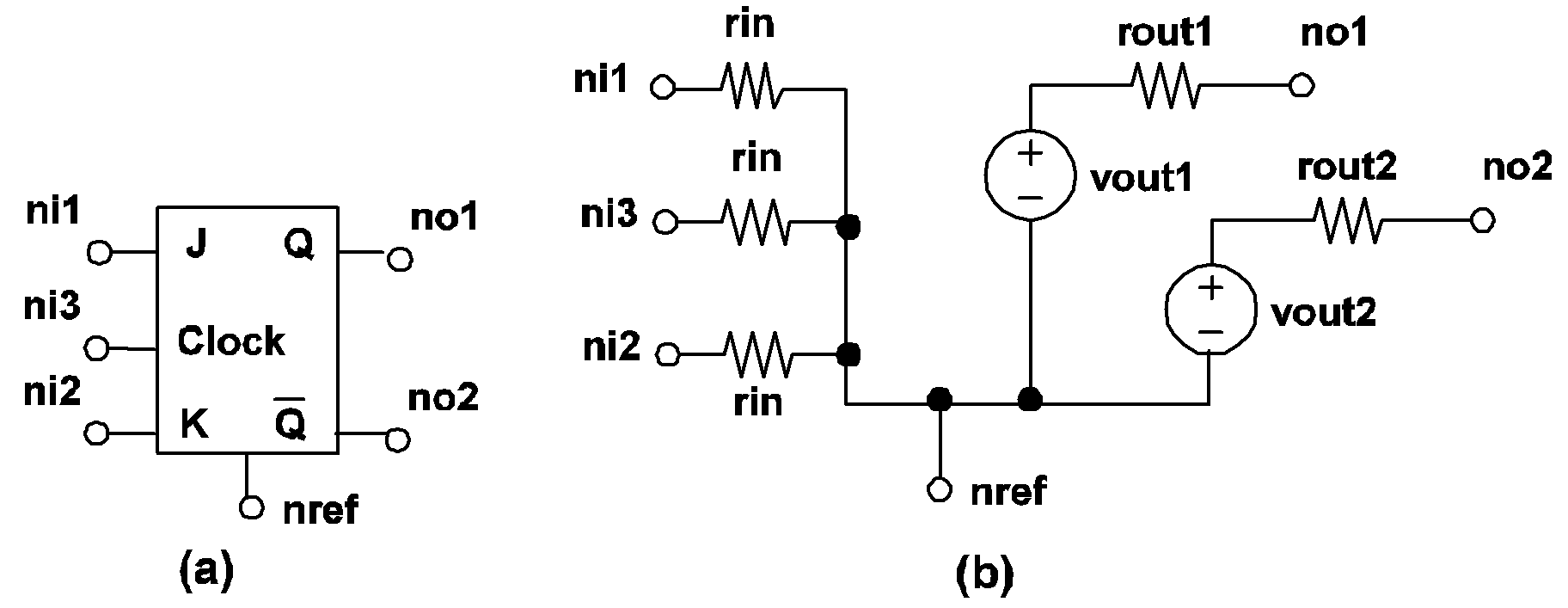 |
4.14 Clocked J-K Flip Flop model: (a) Symbol for a SIMPLIS Clocked J-K flip flop, (b) Model for a SIMPLIS Clocked J-K flip flop. |
Clocked Data Flip-Flop
.MODEL mname CLK_DFF TH=threshold  HYSTWD=hystwd
+ VOL=vol  VOH=voh  RIN=rin  ROUT=rout
+ LOGIC={POS | NEG}  TRIG_COND={0_TO_1 | 1_TO_0}
| .MODEL | is the six-character keyword ".MODEL" |
| mname | is a legal model name as explained in Model Names and Subcircuit Names |
| CLK_DFF | is the seven-character keyword "CLK_DFF" to stand for CLK_DFF-type simple logic gates |
| TH= | is the three-character keyword "TH=" |
| threshold | is a floating-point number which defines the threshold value of the input voltage in volts, which together with hystwd, determines the values of the input voltage at which the input states of the exclusive-OR gate will be changed from a logic 0 to a logic 1 and vice versa |
| HYSTWD= | is the seven-character keyword "HYSTWD=" |
| hystwd | is a positive floating-point number which defines the hysteresis width of the input voltage in volts |
| VOL= | is the four-character keyword "VOL=" |
| vol | is a floating-point number representing the low value of the output voltage in volts |
| VOH= | is the four-character keyword "VOH=" |
| voh | is a floating-point number which defines the high value of the output voltage in volts and must be larger than vol |
| RIN= | is the four-character keyword "RIN=" |
| rin | is a floating-point number which defines the input resistance |
| ROUT= | is the five-character keyword "ROUT=" |
| rout | is a floating-point number which defines the output resistance in ohms |
| LOGIC= | is the six-character keyword "LOGIC=" |
| POS | is the three-character keyword "POS" |
| NEG | is the three-character keyword "NEG" |
| TRIG_COND= | is the ten-character keyword "TRIG_COND=" |
| 0_TO_1 | is the six-character keyword "0_TO_1" |
| 1_TO_0 | is the six-character keyword "1_TO_0" |
If TRIG_COND = 0_TO_1, the clocked data flip-flop is considered to be "triggered" when the logic state of the clock input changes from 0 to 1. Similarly, a logic 1 to logic 0 transition for the clock input is considered to "trigger" this type of flip-flop if TRIG_COND = 1_TO_0. The logic state of each output will not change except at the triggering moment. At the triggering moment, the logic state of the normal output Q will follow the logic state of the data input terminal.
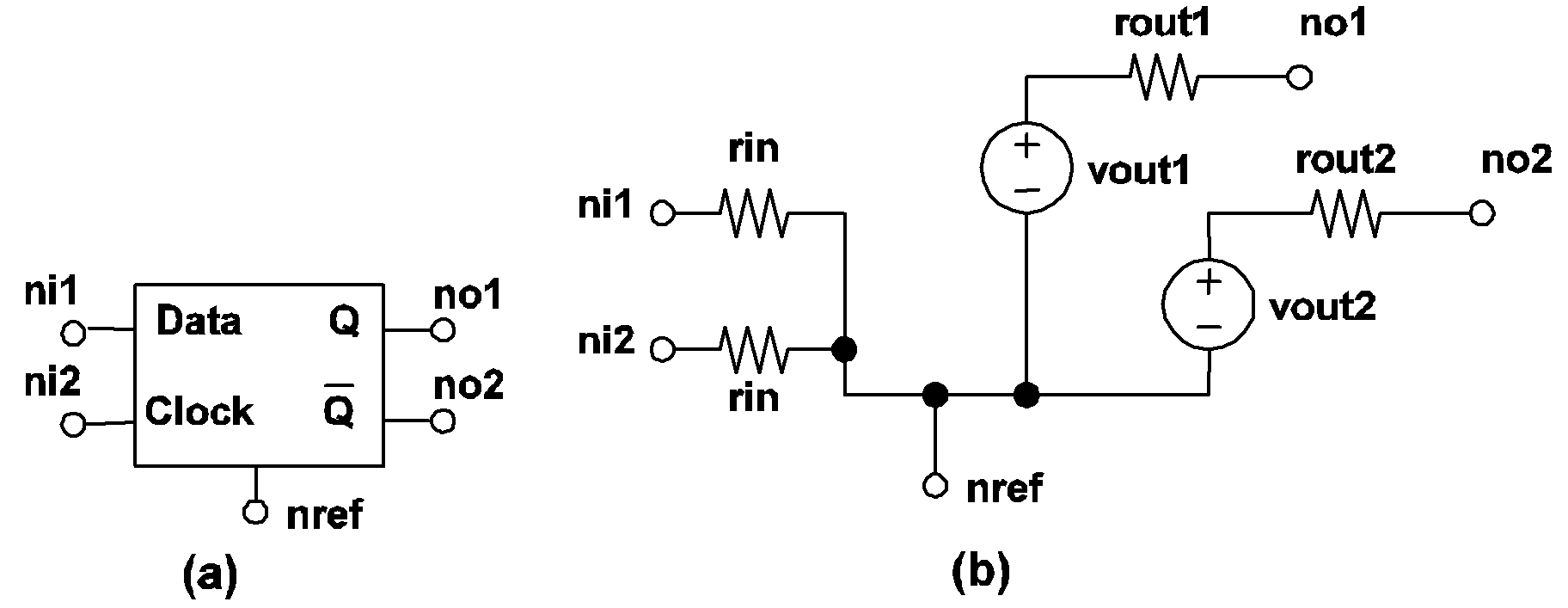 |
4.15 Clocked Data Flip Flop model: (a) Symbol for a SIMPLIS Clocked Data flip flop, (b) Model for a SIMPLIS Clocked Data flip flop. |
Clocked Toggle Flip-Flop
.MODEL mname CLK_TFF TH=threshold  HYSTWD=hystwd
+ VOL=vol  VOH=voh  RIN=rin  ROUT=rout
+ LOGIC={POS | NEG}  TRIG_COND={0_TO_1 | 1_TO_0}
| .MODEL | is the six-character keyword ".MODEL" |
| mname | is a legal model name as explained in Model Names and Subcircuit Names |
| CLK_TFF | is the seven-character keyword "CLK_TFF" to stand for CLK_TFF-type simple logic gates |
| TH= | is the three-character keyword "TH=" |
| threshold | is a floating-point number which defines the threshold value of the input voltage in volts, which together with hystwd, determines the values of the input voltage at which the input states of the exclusive-OR gate will be changed from a logic 0 to a logic 1 and vice versa |
| HYSTWD= | is the seven-character keyword "HYSTWD=" |
| hystwd | is a positive floating-point number which defines the hysteresis width of the input voltage in volts |
| VOL= | is the four-character keyword "VOL=" |
| vol | is a floating-point number representing the low value of the output voltage in volts |
| VOH= | is the four-character keyword "VOH=" |
| voh | is a floating-point number which defines the high value of the output voltage in volts and must be larger than vol |
| RIN= | is the four-character keyword "RIN=" |
| rin | is a floating-point number which defines the input resistance |
| ROUT= | is the five-character keyword "ROUT=" |
| rout | is a floating-point number which defines the output resistance in ohms |
| LOGIC= | is the six-character keyword "LOGIC=" |
| POS | is the three-character keyword "POS" |
| NEG | is the three-character keyword "NEG" |
| TRIG_COND= | is the ten-character keyword "TRIG_COND=" |
| 0_TO_1 | is the six-character keyword "0_TO_1" |
| 1_TO_0 | is the six-character keyword "1_TO_0" |
If TRIG_COND = 0_TO_1, the clocked toggle flip-flop is considered to be "triggered" when the logic state of the clock input changes from 0 to 1. Similarly, a logic 1 to logic 0 transition for the clock input is considered to "trigger" this type of flip-flop if TRIG_COND = 1_TO_0. The logic state of each output will not change except at the triggering moment. At the triggering moment, the logic state of each output remains the same as the logic state before the triggering moment if the state of the toggle input is logic 0. On the other hand, the logic state of each output is complemented if the state of the toggle input is logic 1 at the triggering moment.
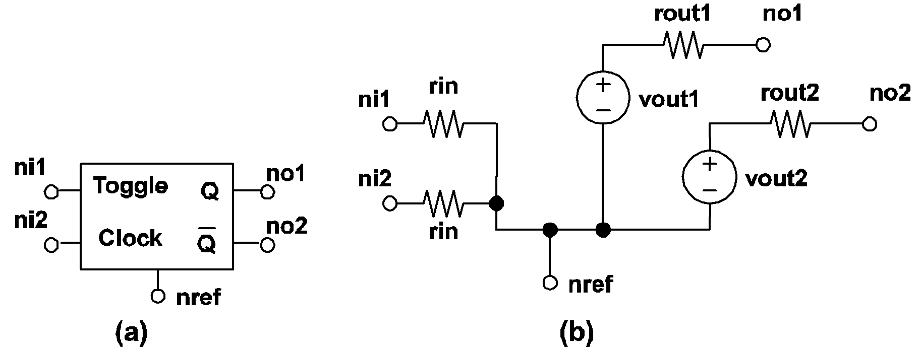 |
4.16 Clocked Toggle Flip Flop model: (a) Symbol for a SIMPLIS Clocked Toggle flip flop, (b) Model for a SIMPLIS Clocked Toggle flip flop. |
Latch
.MODEL mname LATCH TH=threshold  HYSTWD=hystwd
+ VOL=vol  VOH=voh  RIN=rin  ROUT=rout
+ LOGIC={POS | NEG}  ENABLE_LEVEL={0 | 1}
| .MODEL | is the six-character keyword ".MODEL" |
| mname | is a legal model name as explained in Model Names and Subcircuit Names |
| LATCH | is the five-character keyword "LATCH" to stand for LATCH-type simple logic gates |
| TH= | is the three-character keyword "TH=" |
| threshold | is a floating-point number which defines the threshold value of the input voltage in volts, which together with hystwd, determines the values of the input voltage at which the input states of the exclusive-OR gate will be changed from a logic 0 to a logic 1 and vice versa |
| HYSTWD= | is the seven-character keyword "HYSTWD=" |
| hystwd | is a positive floating-point number which defines the hysteresis width of the input voltage in volts |
| VOL= | is the four-character keyword "VOL=" |
| vol | is a floating-point number representing the low value of the output voltage in volts |
| VOH= | is the four-character keyword "VOH=" |
| voh | is a floating-point number which defines the high value of the output voltage in volts and must be larger than vol |
| RIN= | is the four-character keyword "RIN=" |
| rin | is a floating-point number which defines the input resistance |
| ROUT= | is the five-character keyword "ROUT=" |
| rout | is a floating-point number which defines the output resistance in ohms |
| LOGIC= | is the six-character keyword "LOGIC=" |
| POS | is the three-character keyword "POS" |
| NEG | is the three-character keyword "NEG" |
| ENABLE_LEVEL= | is the thirteen-character keyword "ENABLE_LEVEL=" |
If ENABLE_LEVEL = 1, the latch is considered to be "enabled" when the state of the enable input is logic 1. Similarly, if the state of the enable input is logic 0, a latch is considered to be "enabled" if ENABLE_LEVEL = 0. The logic state of the output will not change except when the latch is enabled. When the latch is enabled, the output logic state of the latch follows the logic state of the data input terminal.
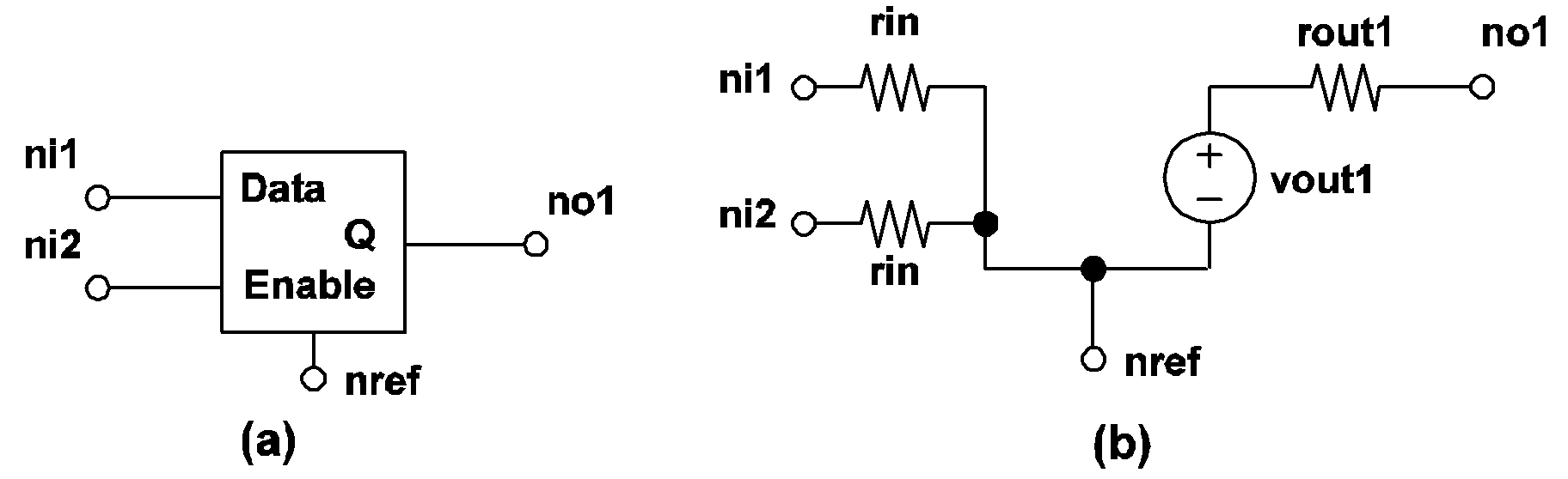 |
4.17 Latch model: (a) Symbol for a SIMPLIS Latch, (b) Model for a SIMPLIS Latch. |
| ◄ Overview | Overview ▶ |