Application C - Low-Voltage High-Current Tuned Load Line Techniques
To download the examples for the Applications Module, click Applications_Examples.zip
In this topic:
What You Will Learn
In this topic you will learn how to use SIMPLIS to tune the dynamic performance of a processor or memory power supply. These high-current very low-voltage power supplies are often called Voltage Regulator Modules (VRMs) if they are prepackaged in module form, or a Voltage Regulator Down (VRD) solution if the design is made up of discrete components laid out directly on the mother board.
We define the term "tuned load line" to mean a DC to DC converter output characteristic where the output voltage drops a specified amount for a given step load current increase with near zero undershoot and for a given step load decrease with near zero overshoot in the dynamic response of the output voltage.
Many voltage regulator architectures exist on the market capable of meeting the requirements. For these exercises, the control architecture features peak current mode control with internal MOSFET current sensing and constant slope compensation. Various multi-phase VRM output inductor-capacitor configurations are analyzed where we vary the amount of ceramic output capacitance and compare the performance of multiple discrete inductors versus a coupled output inductor structure.
We will use SIMPLIS to do the following:
- Model the AC impedance of a ceramic capacitor based on supplier data sheets.
- Perform an AC analysis on a VRM system.
- Evaluate the Transient performance of a VRM system.
- Demonstrate one advantage of coupled inductors versus discrete inductors.
- Plot a VRM system load line.
Model Requirements
- A simple capacitor model test bench will be used to evaluate output capacitor AC impedance.
- A VRM model test bench will be used to evaluate performance based on the number of ceramic output capacitors used in a design.
- Various VRM model test benches will be used to evaluate discrete and coupled output inductor performance.
- A VRM model test bench will be used to evaluate the system load line.
Simplified System Requirements
The following summarizes the VRM system requirements that we will attempt to meet in this exercise.
- Nominal output voltage of 1.00 V at zero load current
- Output voltage versus output current load line impedance of 570 µΩ with a tolerance band of +/-15 µΩ over the load current range
- Voltage regulation tolerance band of +/20 mV over the load line range
- Zero to full load transient of 100A with a di/dt of 100 A/us
- VRM voltage feedback loop bandwidth ~ 200 kHz with 45 degrees of phase margin
- All ceramic output capacitance, 47uF X5R 1206 package preferred
Discussion
The output capacitors are a key to the performance of high frequency multi-phase VRMs. Depending on the control architecture, capacitor technologies can make or break the application. For example, polymer capacitors exhibit a large capacitance value but the ESR is very high compared to an equivalent bank of ceramic capacitors. Load transients that must be sourced by polymer OS-CON output capacitors will show a voltage drop due to ESR and ESL impedances. A typical ESR for a 2.7mF polymer capacitor is 5mΩ. By comparison, a bank of 44 X 47uF X5R ceramic capacitors provides 1.3mF with 68nΩ of ESR and 10pH of ESL.
Printed Circuit Board (PCB) space is at a premium on high performance computing systems, especially surrounding the processors and memory. The main PCB can have 30 layers. A huge amount of effort is put into timing analysis for critical nets. Power and ground are usually run on multiple layers to reduce impedance. Vias need to be in place for connectivity to internal layers without adding impedance. All of these factors make PCB space very expensive. So, anything that can reduce the size of the multiphase power system and still meet the requirements of tight regulation, load line and transient performance and reduce the cost is highly desirable.
A word about transient performance... Depending on the processor technology, Intel vs. IBM vs. AMD all exhibit a certain amount of leakage through the silicon structures. Some of the technologies exhibit a cubic change in current for an incremental change in supply voltage. This effect is what drives the need to minimize overshoot during transient unloading or processing operations. Removing the overshoot characteristics will reduce the temperature of the processor core and improve battery life for portable devices. A well designed power system load line helps to improve this effect by lowering the output voltage as the load current increases and raising the output voltage as the load current decreases. Increasing the slope of the load line or the droop will reduce the bandwidth required to achieve an acceptable phase margin but reducing the bandwidth has the disadvantage of slowing down the feedback loop.
In the next two exercises we create a simple SIMPLIS model for a ceramic capacitor and then compare it to the parameters in the manufacturer's data sheet.
Exercise #1: Ceramic Capacitor Model Characterization
Murata maintains a website for their discrete components. Included is a tool called SimSurfing for generating device models. The Murata ceramic capacitor model is a far more complex model than the simple model required. You can extract the data to make simple model from the SimSurfing output. Murata data at 1MHz and a DC bias voltage of 1V was used for the simpler SIMPLIS model. Ceramic capacitors provide for output filtering with the smallest size, lowest ESR and ESL. Ceramic capacitor parasitic features begin to become insignificant above ~1 MHz. You will use the parasitic values at ~1MHz for ESR & ESL. For the capacitance value you will use a value that matches the Murata impedance curve with 1 volt DC bias. Voltage regulator band width can be optimized by tuning the amount of ceramic output capacitance. The package size used will be 1206.
To access the SimSurfing Tool, click on Murata SimSurfing Tool.
Next, you will run a simulation to characterize the impedance of the ceramic output capacitor to be used in our VRM model.
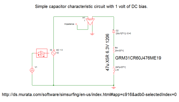
- Open schematic apps_c_1_capacitor_impedance.sxsch.
Below is shown the schematic of the capacitor test bench:
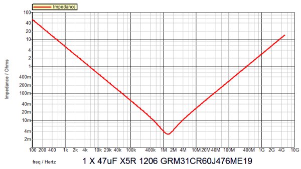
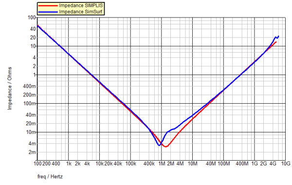
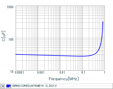
- Run the AC analysis simulation for the ceramic output capacitor. Result: Below is the AC impedance plot for one ceramic capacitor. Of note is the -20db/decade slope up to ~1MHz, capacitance of 30uF, ESR of 3mohm and ESL of 447pH.
Exercise #2: Compare SIMPLIS model to Murata SimSurfing Data
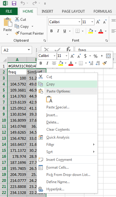
- Access the SimSurfing .csv data, click: SimSurf Data GRM31CR60J476ME19
- Save the .csv file.
- Open the .csv file with Excel.
- Change cell A2 to "freq", change cell B2 to "SimSurf".
- Copy the two columns of frequency and capacitor impedance data onto your clip
board.
- Paste these data to the capacitor impedance graph in SIMetrix/SIMPLIS by clicking
"Paste ASCII Data".
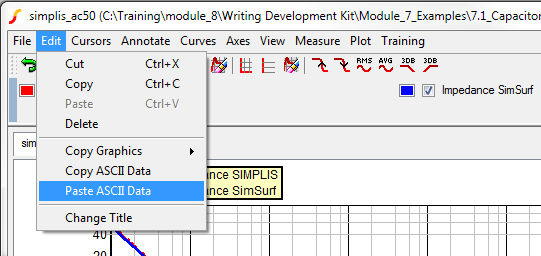
- Compare the supplier data to the SIMPLIS model. Is the data reasonably
accurate?Result: Below is the AC impedance plot for one ceramic capacitor, modeled in SIMPLIS (red) and extracted .csv data overlaid from the Murata SimSurf tool (blue). Of note is the -20db/decade slope to ~1MHz, capacitance of 30uF, ESR of 3mohm and ESL of 447pH.
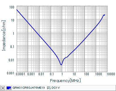
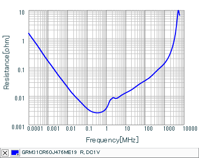
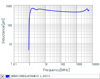
For your reference below are the AC impedance, AC resistance, AC inductance and AC capacitance versus frequency plots for the 47uF 1206 capacitor GRM31CR60J476ME19 from the manufacturer's SimSurfing database.
Discussion
The assembled simple ceramic capacitor model seems adequate for the VRM output filter although not exact at frequencies above ~1MHz. The VRM will require a bandwidth of over 100kHz and so a single-pole capacitor transfer function to ~1MHz is desirable to optimize the voltage feedback loop. Because we are using a peak-current control scheme, and with these ceramic capacitors on the output, the power stage modulator exhibits a single-pole transfer function. As a result, a passive non-reactive compensator is all that is required to close the voltage feedback loop given the single pole power stage transfer function. Consequently, the compensator transfer function does not contribute to over/undershoot and exhibits a flat gain characteristic over the frequencies of interest.
Next you will examine the performance of the VRM with the assembled ceramic capacitor model. The following exercises will demonstrate VRM loop gain, transient response and load line with various amounts of capacitance and values of output inductors.
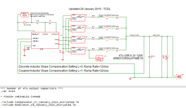
Discrete inductors will be simulated initially. Later we will replace these four discrete inductors with a coupled inductor structure and compare the performance of these two design approaches for magnetic energy storage in this VRM application.
Below are links to supplier datasheets from which the fixed discrete inductor model used herein were referenced. Multiphase VRM inductors usually have only one turn. The permeability of the core material is varied to achieve different inductance values with single turn structure. As an example, the © COOPER core exhibits a common surface mount package and footprint. Only the K-factor varies depending on the desired inductance and saturation current. The inductor could be modeled with a PWL inductor that would reduce in inductance with increased current. For this exercise a fixed inductor was chosen for simplicity and ease of comparison. Some companies will custom make inductors to your application. Many, many more discrete inductors exist on the market.
Exercise #3: VRM example demonstrating POP, AC and Transient analysis with discrete inductors
The simulation you will run is to characterize the VRM stability and transient response with the capacitor model developed above and discrete 150nH inductors.
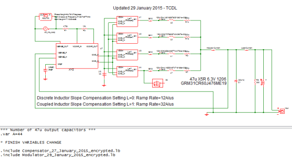
- Open schematic apps_c_2_discrete_inductor_44x.sxsch.
- Run the simulation for the VRM model.
- Review the simulation results for bandwidth, phase margin and transient response.
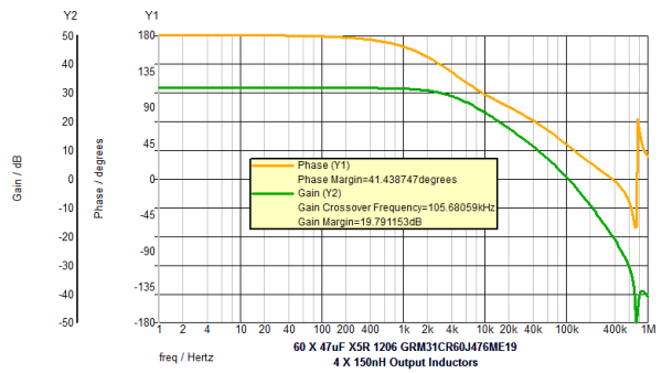
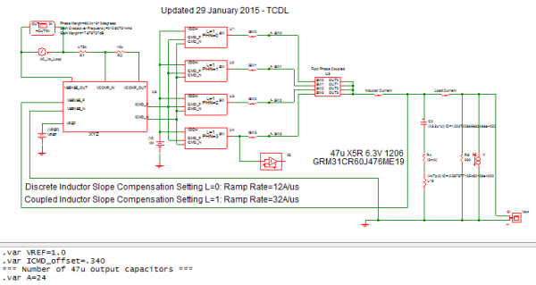
Below is the schematic of the VRM test bench. The output inductor is 150nH and the output capacitance is 44 pieces 47uF.
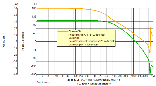
Discussion
Looking at the voltage overshoot, we see that the 150nH inductor has significant amount of energy stored 1/2Li2 when the load is removed. Reducing the output inductor to 100nH will reduce this stored energy when the load is removed. Increasing the output capacitance will also reduce the output voltage overshoot due to the transient unloading energy. However, if PC board space is very tight, it may be undesirable to increase the capacitance. These are all trade-offs the designer makes, and SIMPLIS is a very powerful tool for exploring the many design options.
In the next exercise, let us assume you do have the board space to increase the output capacitance footprint. The efficiency of the VRM is higher with the 150nH inductor than with a 100nH inductor due to the lower AC ripple current.
Exercise #4: VRM example demonstrating increased output capacitance from 44 pieces to 60 pieces 47uF
The simulation you will run in this exercise is to characterize the VRM stability and transient response with increased output capacitance.
- Open schematic apps_c_3_discrete_inductor_60x.sxsch.
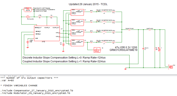
- Run the simulation for the VRM model.
- Review the simulation results for bandwidth, phase margin and transient response.
Below is the schematic of the VRM test bench. The output inductor is 150nH and the quantity of 47uF output capacitors is 60 pieces.
Discussion
The previous simulation with 150nH inductors and 44 pieces 47uF lacked performance with margin but nearly met the requirements. A 100nH inductor has less 1/2Li2 at the unloading event. Let's assume our project management refuses to give us the extra board space. You are told you could be a bit less efficient. you are told form factor and size are a premium for this program. A 100nH inductor is the same size and footprint as the 150nH inductor with slightly different core permeability. You are asked to figure out how to make the solution work with 44 pieces of 47uF capacitors or less.
Exercise #5: VRM example demonstrating the performance with an output inductance of 100nH per phase and total of 44 output ceramic capacitors of 47uF each.
The simulation you will run is to characterize the VRM stability and transient response.
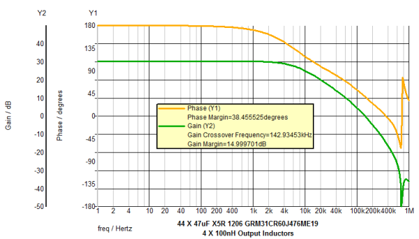
- Open schematic apps_c_4_discrete_inductor_100n.sxsch.
- Run the simulation for the VRM model.
- Review the simulation results for bandwidth, phase margin and transient response.
Below is the schematic of the VRM test bench. The output inductor is 100nH and the 47uF quantity is 44 pieces.
Discussion
We still have one more trick up our sleeve... the coupled inductor.
Coupling all the output inductors together can provide a superior level of performance compared with the discrete inductor approach. This approach can also provide a higher level of power density.
We next look at this is a very complex system with a complex coupled magnetic circuit inserted into a 4-phase synchronous buck topology. SIMPLIS is an excellent tool to understand the resulting performance trade-offs that are not easily analyzed by hand. The coupled inductor used in the next exercise is a "ladder structure" where each winding is wound around one rung of the ladder core. This particular core structure has certain features that have been patented by Maxim/Volterra and their patent is among the reference materials listed below that address the general theory of this device.
Below are links to supplier datasheets and general information from which the model used in the next 3 exercises was constructed.
- Coupled Inductors © VITEC
- Coupled Inductors © COOPER
- Maxim/Volterra Patent on a Coupled Inductor Structure
- Coupled Inductors Volterra
- Coupled Inductors APEC 2002
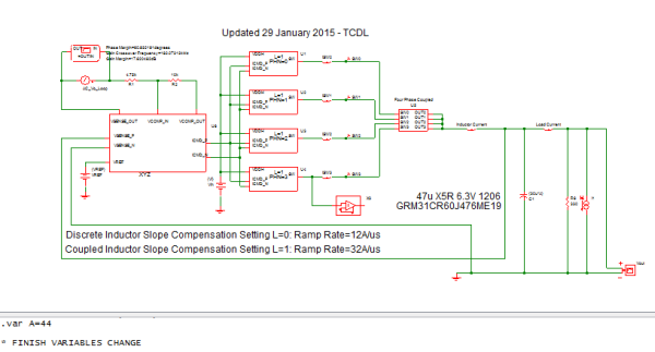
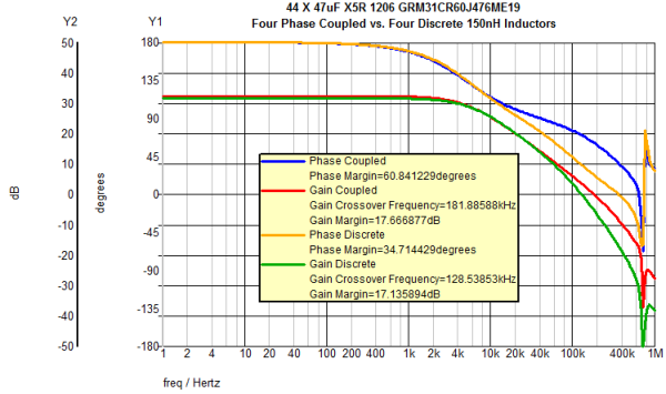
Exercise #6: VRM example demonstrating coupled inductor performance with 44 output ceramic capacitors of 47uF each
The simulation you will run is to characterize the VRM stability and transient response.
- Open schematic apps_c_5_coupled_inductor_44x.sxsch.
- Run the simulation for the VRM model.
- Review the simulation results for bandwidth, phase margin and transient response.
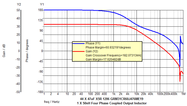
Below is the schematic of the VRM test bench. The output inductor is a four phase coupled inductor with 44 pieces of 47uF
Exercise #7: VRM example demonstrating detailed coupled inductor performance
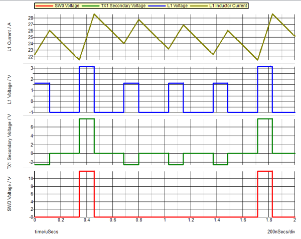
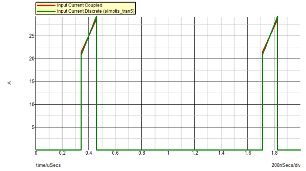
The simulation you will run is to provide a deeper understanding of the coupled inductor structure. The coupled inductor structure will be explored for "internal" voltage and current waveforms.
- Open schematic apps_c_6_coupled_inductor_detailed.sxsch.
- Open schematic apps_c_7_discrete_inductor_detailed.sxsch.
- Run both simulations for the VRM models.
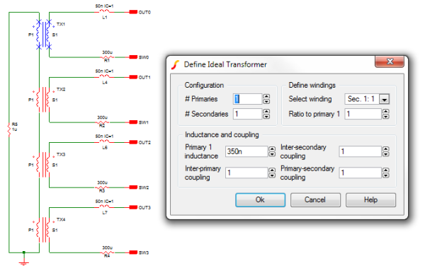
- Descend the hierarchy for the coupled inductor.
- Review the simulation results for coupled inductor voltages and currents.
Below is the schematic of the model of a four phase coupled inductor sub-circuit. The four transformers each have a coupling coefficient of one and a magnetizing inductance of 350nH. The function of the transformer primaries in series is to model the magnetic coupling of each of the four windings of the coupled inductor. Now each of the four phase currents are magnetically coupled to each other, thereby providing a degree of phase-to-phase current sharing. The accompanying materials listed above discuss the theory behind this model.
Exercise #8: VRM example demonstrating load line regulation performance
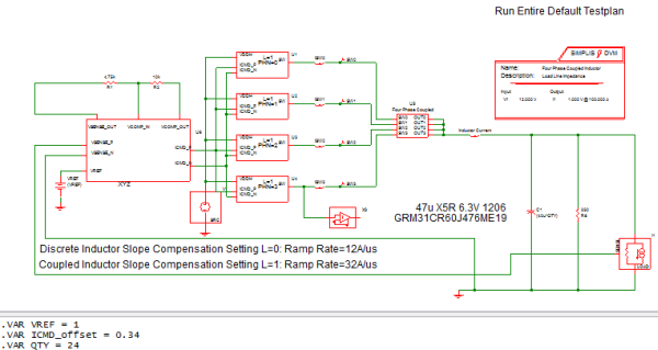
The next simulation you will run is to plot the power supply load line characteristic using SIMPLIS DVM. The DVM schematic has been pre-configured for you. This testplan runs six POP simulations on the converter, each simulation then measures the DC output voltage and current. A final test aggregates the results and plots the points on an XY graph.
- Open schematic apps_c_8_coupled_inductor_load_line_DVM.sxsch.
- Run the simulation for the VRM model by clicking DVM | Run | Run Entire
Schematic's Default Testplan
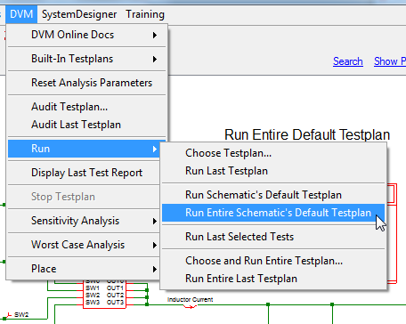 Result: The testplan will run.
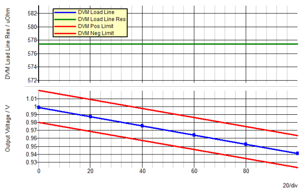
 - Review the simulation results for a 570µΩ load line impedance +/-15 µΩ.
Below is the schematic of the four phase coupled inductor VRM with the DVM Load and Source to plot load line.
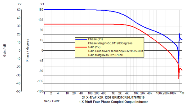
Exercise #9: VRM example demonstrating a four phase coupled inductor with 24 pieces of 47uF
The last simulation you will run is to characterize the VRM stability and transient response. This simulation will demonstrate how low the output capacitance can be with coupled inductor topology. Recall that with a discrete 100nH inductor you needed ~44 X 47uF capacitors and you still had 33mV of overshoot.
- Open schematic apps_c_9_coupled_inductor_24x.sxsch.
- Run the simulation for the VRM model.
- Review the simulation results for bandwidth, phase margin and transient response.
Below is the schematic of the VRM test bench. The output inductor is a four phase coupled inductor with 24 pieces of 47uF.
Conclusions and Key Points to Remember
- Ceramic capacitor characteristics were modeled using supplier data sheets and then applied to the VRM model.
- Performance differences between four discrete inductors and a four phase coupled inductor were modeled.
- Coupled inductors offer a high level of performance with a small physical footprint.
- SIMPLIS provides an effective tool to tune processor or memory VRM/VRD (Voltage Regulator Module/Voltage Regulator Down) solutions.
- SIMPLIS provides an effective tool to analyze the coupled inductor internal waveforms.
- Shown below are the performance comparisons between the various simulations for the
preceding exercises:
Inductor Type Inductance (H) 47uF QTY Undershoot (mV) Overshoot (mV) Bandwidth (Hz) Phase Margin(°) Discrete 150n 44 < 2 76.5 129k 34.8 Discrete 150n 60 < 2 42.8 105k 41.4 Discrete 100n 44 < 2 33.0 143k 38.5 Coupled 50n 44 < 10 < 2 182k 61 Coupled 50n 24 < 10 < 2 210k 60